The Use of Laser Scanning Confocal Microscopy (LSCM) in Materials Science
Laser scanning confocal microscopes are essential and ubiquitous tools in the biological, biochemical, and biomedical sciences, and play a similar role to scanning electron microscopes in materials science. However, modern laser scanning confocal microscopes have several advantages for the characterization of materials, in addition to their obvious uses for high resolution reflected and transmitted light optical microscopy. Herein, we provide several examples that exploit the laser scanning confocal microscope’s capabilities of pseudo-infinite depth of field imaging, topographic imaging, fluorescence imaging, and photo-stimulated luminescence imaging for the characterization of different materials.
Introduction
Confocal microscopy is a ubiquitous technique in the life sciences, as it provides precise optical sectioning of fluorescently labeled thick specimens. To date, however, it has been underutilized in materials science. Recent advances in both instrumentation and computing power now make confocal microscopy an attractive imaging and analytical tool for materials scientists. When properly configured, a confocal microscope can serve as a high-resolution optical microscope (in either transmission or reflection) with ‘infinite’ depth of field, while at the same time serving as a non-contact optical profilometer. Combined and synchronized with an external spectrometer, techniques such as photo-stimulated luminescence spectroscopy are enabled.
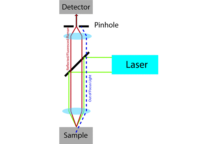
Though the confocal microscope was invented in 1955 by Minsky, [1] the widespread use of confocal imaging was not possible until the invention of lasers and the availability of significant computing power. [2-6] Laser scanning confocal microscopes (LSCMs) use collimated laser light as a ‘point’ illumination source, with point focus on the sample, and focus the reflected, transmitted, or fluoresced light through a pinhole to provide a ‘point’ detector. The pinhole defines a second crossover focal point and serves as a wide-angle filter to the detector. If scattered light does not pass through the pinhole, then it is not in focus. Once the light passes through the pinhole, it is typically split into different wavelengths using dichroic mirrors and filters, and then detected by photomultiplier tubes (PMTs). Imaging of large areas of the sample is achieved by raster scanning the beam across the sample using mirrors controlled by piezoelectric actuators (Figure 1).
This paper is arranged as follows. The equipment is briefly described, after which several examples using different imaging modalities that exploit the advantages of confocal microscopy are shown. The advantage of using a hot stage in a confocal microscope, and of adding a high-resolution spectrometer for photo-stimulated luminescence imaging is also addressed.
Methods
All of the data presented in this paper were obtained with an Olympus FV1000 filter-based confocal scan head coupled to an Olympus BX62 upright motorized microscope (Olympus Corp., Tokyo, Japan). Four lasers provide a total of six different wavelengths (405, 458, 488, 514.5, 543, and 633 nm), which can be combined into a single beam before imaging. For reflected light imaging, we prefer the 405 nm laser, as the optical resolution is directly proportional to wavelength.
The FV1000 scan head is equipped with three PMTs for reflected/fluoresced light, one PMT for transmitted (non-confocal) light, an Acton 2300i 0.3 m spectrometer (Princeton Instruments, Acton, MA, U.S.A.) equipped with a Princeton Instruments PIXIS 100BR backilluminated, deep depletion, thermoelectrically cooled charge-coupled device detector (Princeton Instruments, Trenton, NJ, U.S.A.).
Results and Discussion
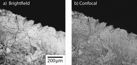
Traditionally, to get the highest lateral resolution from a metallurgical microscope, samples had to be polished to a high degree of flatness and then lightly etched to provide optical contrast. If the sample was not perfectly flat or was over-etched, it became difficult or impossible to obtain high-quality optical images. With conventional brightfield optical microscopy, in-focus regions are crisp and clear, whereas out-of-focus regions are less distinct. [7] In confocal microscopy, in-focus regions are similarly crisp and clear, but the intensity in out-of-focus regions drops rapidly. [2-4] As a result, little to no signal is obtained from out-of-focus regions.
When combined with a motorized focusing mechanism, it is relatively simple to take a series of images at different focal planes and form a composite image to obtain an ‘infinite depthof-field’ image. For a well-prepared metallographic sample, such as the polished PH13– 8Mo martensitic stainless steel shown in Figure 2, the confocal image is noticeably sharper, but the actual increase in resolution is modest.
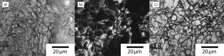
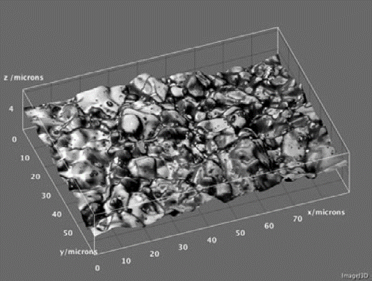
Confocal microscopy has much more significant advantages for samples that cannot be polished to a flat surface. For example, the surface of a sintered aluminum oxide (Al2O3) sample was imaged without further specimen separation using brightfield optical microscopy, and it is difficult to resolve the microstructure clearly because of the narrow depth of field of a high numerical aperture objective (Figure 3a). With laser scanning confocal imaging, however, the depth of field becomes slightly smaller, but the out-of-focus regions are dark (Figure 3b). Multiple images can be obtained over a range of focal planes; collecting all the in-focus data and combining the maximum intensity pixels yields an essentially infinite depth-of-field image (Figure 3c).
Further, in the process of obtaining adequate images to provide an infinite depth-of-field micrograph, sufficient information is also gathered to produce a topographic map of the sample surface (Figure 4).
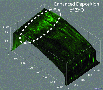
For materials scientists, many ceramics, semiconductors, and polymeric materials can provide strong fluorescence, although metals do not fluoresce. By using multiple PMTs, wavelength-specific dichroic mirrors, and bandpass wavelength filters in front of the PMTs, it is possible to image with reflected and fluoresced light simultaneously. An example of this is given in Figure 5, where a piston ring removed from an engine was imaged using both reflected and fluoresced light. The lubricant from the engine deposited ZnO on the piston ring, which is visible as a green fluorescent signal when imaged with the 405 nm laser. By simultaneously imaging with both the reflected laser and the fluoresced radiation, it is possible to obtain a topographic image (from reflected light) and two infinite depth-of-field images (from reflected and fluoresced light, respectively). The infinite depth of field fluorescence image shows a bright band corresponding to increased ZnO deposits. By taking a 3D model of the surface and applying the fluorescence image as a texture, it is possible to see clearly where the greatest deposits of ZnO occurred.
a-alumina (a-Al2O3) has strong fluorescence in response to visible laser illumination if trace quantities of chromium are present. In practice, this means that any a-alumina samples, short of a semiconductor-grade sapphire wafer, fluoresce under laser irradiation. This fluorescence is known as the ‘ruby’ fluorescence and occurs as a peak doublet around 693 nm, known as the R1/R2 doublet. The specific wavelengths of the two peaks are stress-sensitive, with the R2 peak being sensitive only to the trace of the stress tensor. The R2 peak shift of ruby has long been used to calibrate the pressure in diamond anvil cells, and the piezospectroscopic coefficients are well established. [8-10] Via spectroscopic analysis of photo-stimulated luminescence in LCSM measurements, stress maps of materials surfaces can be generated, which we call confocal photo-stimulated microscopy (CPSM). [10]
Platinum-modified nickel aluminide (b-phase NiPtAl alloys) bond coats on Ni-base single crystal superalloys have been the subject of extensive studies because of the propensity of these coatings to ‘rumple’ upon thermal cycling. [1116] This rumpling can increase the heat transfer from the thermal barrier coating to the underlying metal substrate, accelerating the degradation of structural components. It has also been predicted that the rumpling may affect the stresses in the thermally grown oxide (TGO), leading to premature spallation of the thermal barrier coating. Previous modeling using finite element analysis had predicted that large stress variations would be present due to topography of the TGO, with ‘peaks’ being less compressive and ‘valleys’ being more compressive. [17,18] A NiPtAl bond coat on a René N5 superalloy was thermally cycled for 24 one-hour cycles at 1100 °C (2012 °F). A topographic map was obtained by operating the LSCM instrument in reflected-light mode. A series of images were taken at various focal planes to reconstruct the surface topography (Figure 6b). Without moving the sample, a CPSM stress map was obtained (Figure 6a). Comparing Figure 6a to 6b, a correlation is evident between the topography and the residual stress in the TGO. This can be confirmed by using the topographic data to create a 3D model of the surface.
The stresses measured from the same region can then be projected onto this surface as a texture, and as shown in Figure 7, an apparent correlation between topography and residual stress is obtained. The stresses are less compressive in the areas with downward curvature and more compressive where the curvature is upward, providing agreement with previous finite element models. [17,18]
A hot stage attachment is a useful addition to LSCM. Generally, with high-temperature optical imaging, incandescence significantly degrades the image quality. With LSCM, a short wavelength of 405 nm laser can be used for imaging; combined with wavelength filters in the detector section, incandescence can be eliminated. The result is image quality at elevated temperatures that is equivalent to that at room temperature.
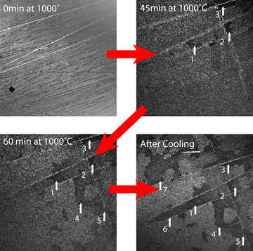
An example of hot stage imaging on our LSCM is shown in Figure 8. A g-phase NiCrAl alloy was oxidized at 1000 °C (2012 °F) and held for 60 min. Upon reaching the oxidation temperature, a ‘reaction front’ was observed to progress across the surface. At the conclusion of the experiment, the hot stage was cooled at 100 °C min-1 (212 °F min-1) to freeze in the feature of interest. As can be seen in Figure 8, the reaction front progressed only modestly as the sample returned to room temperature.
Conclusions
In conclusion, the confocal microscope is a very useful tool for materials scientists. The microscope can provide the pseudo-infinite depthof-field imaging of a scanning electron microscope, without the need for a vacuum system or the coating of non-conductive samples. At the same time, topographic capabilities of a profiliometer or atomic force microscope are possible, along with fluorescence imaging, and photo-stimulated luminescence spectroscopy (the CPSM mode). These capabilities make the confocal microscope a versatile addition to the materials science characterization toolkit.
References
This text is a digest version of:
Hovis, D. and Heuer, A. (2010), The use of laser scanning confocal microscopy (LSCM) in materials science. Journal of Microscopy, 240: 173-180. doi:10.1111/j.1365-2818.2010.03399.x
[1] M. Minsky, Scanning 1988, 10, 128–138.
[2] D.K. Hamilton, T. Wilson, Appl. Phys. B-Photo. 1982, 27, 211– 213.
[3] K. Carlsson, P.E. Danielsson, R. Lenz,
A. Liljeborg, L. Majlof, N. Aslund, Opt. Lett. 1985, 10, 53–55.
[4] K. Carlsson, N. Aslund, Appl. Optics 1987, 26, 3232–3238.
[5] G. Q. Xiao, T.R. Corle, G.S. Kino, Appl. Phys. Lett. 1988, 53, 716–718.
[6] W. Amos, J. White, Biol. Cell 2003, 95, 335–342.
[7] R.C. Gifkins, Optical Microscopy of Metals, American Elsevier Publishing Company, Inc., New York 1970.
[8] L. Grabner, J. Appl. Phys. 1978, 49, 580–583.
[9] J. He, D.R. Clarke, J. Am. Ceram. Soc. 1995, 78, 1347–1353.
[10] D.B. Hovis, A.H. Heuer, Scr. Mater. 2005, 53, 347–349.
[11] P.K Wright, A.G. Evans, Curr. Opin. Solid State Mater. Sci. 1999, 4, 255–265.
[12] V.K. Tolpygo, D.R. Clarke, Acta Mater. 2000, 48, 3283–3293.
[13] V.K. Tolpygo, D.R. Clarke, Acta Mater. 2004, 52, 5115–5127.
[14] V.K. Tolpygo, D.R. Clarke, Acta Mater. 2004, 52, 5129–5141.
[15] A.G. Evans, D.R. Mumm, J.W. Hutchinson, G.H. Meier, G.S. Pettit, Prog.
Mater. Sci. 2001, 46, 505–553.
[16] D.R. Mumm, A.G. Evans, I.T. Spitsberg, Acta Mater. 2001, 49, 2329–2340.
[17] C.H. Hsueh, J.A. Haynes, J.A.,
M.J. Lance, P.F. Becher, M.K. Ferber,
E.R. Fuller, S.A. Langer, W.C. Carter,
W.R. Cannon, J. Am. Ceram. Soc. 1999, 82, 1073–1075.
[18] C.H. Hsueh, E.R. Fuller, Mater. Sci. Eng. A 2000, 283, 46–55.
Copyright
DOI: 10.1111/j.13652818.2010.03399.x; D. B. Hovis, A. H. Heuer; Journal of Microscopy
© 2010 The Authors Journal of Microscopy © 2010 The Royal Microscopical Society