Film Adhesion of Flexible Electronics Influenced by Interlayers
As flexible electronics emerge for applications such as medical sensors and foldable displays, there is a need to understand the interfacial behavior between the conducting elements and the compliant polymer substrate that the devices are prepared on. Compression-induced delamination is a technique that uses the buckling dimensions to evaluate the interfacial adhesion of materials on flexible substrates quantitatively. This study shows that spontaneous buckles are formed in gold (Au) films, which are deposited without an interlayer. Conversely, external loading is required to delaminate the Au film with the tantalum (Ta) adhesion layer indicating higher adhesion energy.
Introduction
Flexible devices and sensors are an emerging field in the electronics sector used for various applications, such as foldable displays [1,2] and neural electrodes. [3,4] The primary goal in the design of flexible electronics is to achieve significant strain (>10%) without losing electronic functionality. Many designs to achieve this goal consist of small islands of rigid electronics placed on a flexible polymer substrate and connected using metallic lines. In this design, the adhesion between the lines and the underlying substrate is of great importance to device reliability.
The failure of flexible electronic materials occurs via two mechanisms; the fracture of the metallic conducting components through thickness crack formation or the metallic layers delaminate from the substrate. Several testing techniques have been used to analyze cracking failure, the most popular being tensile straining [5–9] and bending. [10–13] The techniques used to evaluate the adhesion of thin films to rigid substrates have advanced our understanding of adhesion and its mechanisms. [14–19] These methods work well for films on rigid substrates; however, flexible electronics present more challenges, and the methods and models for rigid substrates cannot always be employed. Therefore, tensile-induced delamination [20,21] or compression-induced buckling methods [22,23] have been developed to this end. These techniques work well for brittle films, [24–26] but require an extensive amount of straining for ductile films [27] or an overlayer to induce delamination at lower levels of strain. [28,29]
Noble metals, such as Au or Ag, are the materials of choice for the connecting lines between the semiconducting islands. It is advantageous to use these metals because they are ductile, have a low electric resistance, and can be easily deposited and patterned. Unfortunately, these metals, sometimes, have trouble adhering to the polymer substrates used in flexible electronics. Therefore, interlayers, like titanium (Ti), tantalum (Ta), and chromium (Cr), are used to improve the adhesion of the noble metal to the polymer substrate. [26,27,30] Since the conducting metals used are duc tile, methods that can induce defined areas of delamination are desired to determine the effect of interlayers on adhesion energy. Buckling-based techniques are ideal because plastic deformation is minimized, and buckle delamination is well understood. [31–33] Spontaneous buckling can occur when the residual stress of the film is large and compressive, typically in the range of 0.5 GPa – 2 GPa, but typically does not occur on polymer substrates because the substrate can accommodate the film stress by macroscopically bending. Conversely, tensile-induced delamination is effective at creating buckles in a ductile film system of 50 nm Cu with a 10 nm Cr interlayer. [26]
In this work, compression-induced delamination will be used to cause a 300 nm Au film to buckle upon unloading rather than during loading. Buckling during tensile unloading was compared to spontaneous buckling and used to measure the adhesion energy. With the proper utilization of the different buckling phenomena, the adhesion energy of the interface and how much the addition of interlayers improves adhesion can be quantified.
Methods
Au films (300 nm thick) were sputter-deposited with and without a 10 nm Ta interlayer using a DC Magnetron system onto 50 mm thick Kapton polyimide (PI) substrates. [3,34] The Ta film was used as an interlayer to improve the adhesion between Au and PI.
To measure the buckle dimensions, two different devices were used—atomic force microscopy (AFM, Veeco Dimension AFM) and 3D confocal laser-scanning microscopy (CLSM, Olympus LEXT OLS4100 microscope). The CLSM measurements were performed using a laser-wavelength of λ = 405 nm. Because its maximum lateral image size is 80 µm × 80 µm and the vertical limit is 6 mm, the AFM was used only to image smaller buckles. The CLSM can be used to measure all buckle sizes since its vertical limit depends on the distance of the objective to the sample. Gwyddion was used to analyze the images and measure the dimensions of the buckles.
[35] Additionally, focused ion beam (FIB) crosssectioning and scanning electron microscopy (SEM) was used to characterize the buckles.
The buckle dimensions are directly related to the critical buckling stress and the delamination stress of the film at the interface. The stresses and the interfacial fracture energies can be calculated using the well-known Hutchinson and Suo model. [31] The method is based on the Euler beam theory. The critical buckling stress, σb, and the driving stress, σb, can be calculated by using Equations (1) and (2).

where δ is the buckling height, b is the half buckle width, h is the film thickness, E is the film’s elastic modulus, and ν is its Poisson’s ratio. The critical buckling stress is the stress necessary to cause film delamination, and the driving stress propagates the buckles. The interfacial fracture energy,Γ(Ψ), for spontaneous buckles is given by Equation 3 and is used to calculate the adhesion energy of the interfaces.

Results and Discussion
The Au films on PI (without Ta) delaminated spontaneously at the metal-polymer interface in the form of straight-sided and telephone cord buckles due to the high compressive residual stress in the films, whereas, the Au–Ta films on PI did not delaminate. The typical height and length of the spontaneously formed buckles were on the order of hundreds of nanometers to a few micrometers, respectively.
Therefore, a loading-unloading experiment was performed on the Au–Ta films on PI to create buckles to access the adhesion energy. After straining to a maximum strain of 15% and unloading, straight buckles perpendicular to the straining direction were observed (Figure 1). Typically, buckles form parallel to the straining direction when tensile-induced delamination is used because compressive stress builds up due to the difference in the Poisson’s ratio between film and substrate. [20,36] The appearance and spacing of the buckles perpendicular to the straining direction are similar to the cracking of brittle films under tension.
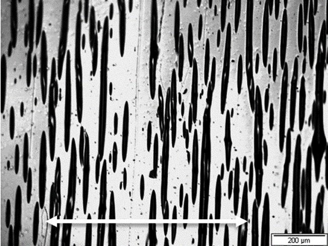
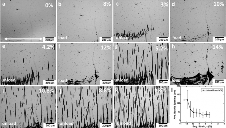
To determine the amount of strain required to cause buckling, incremental load-unload testing was. The loading varied between 2% and 14% strain, while the unloading segments always went to 2N. Optical micrographs were taken at the peak strains and every 1% decreasing strain during unloading (Figure 2a-k). As shown in Figure 2a at 0% strain, no buckles are observed. Upon straining, the film is mostly flat, however small buckles parallel to the straining direction are visible at a preexisting defect in the film. Upon unloading, buckles perpendicular to the straining direction are observed. At lower strains, they are mostly clustered at a series of scratches, but with the increasing strain, the buckles encompass the entire visible area. With each increasing load step, existing interface cracks grow, or more are nucleated which, in turn, produces more buckles upon unloading. Figure 2i–k shows how buckles form and that the density increases during the removal of the tensile load. Finally, Figure 2l shows the measured buckle spacing as a function of the unloading from 14% strain. The buckle spacing during unloading follows the same trend as crack spacing during tensile loading, where the spacing decreases until a plateau is reached at approximately 7% unloading strain. Therefore, it was determined that approximately 6% – 8% maximum strain is required to cause delamination upon unloading.
The spontaneous buckle dimensions were measured by AFM (Figure 3a) and CLSM (Figure 3b) to calculate the adhesion energy of the Au film on PI. Figure 3b shows that the delamination starts as single straight-sided buckles and then continues to propagate as telephone cord buckles. This is a common delamination process in biaxially stressed films with spontaneous buckles because of the large shear stress. [37,38] The buckles in the white box (Figure 3b) are the same as in Figure 3a. The same seven single buckles were measured with both imaging methods. CLSM can image a larger area, and it is possible to measure more buckles from a single image. The height of the buckles varies, and the telephone cord buckles are much taller than the single buckles, more than 5 µm in height. Therefore, AFM cannot measure most of the telephone cord buckles due to the maximum deflection limit of the cantilevers. The sample height for the CLSM is only limited to the distance of the objective to the sample, which is a few millimeters. The marked profiles indicate where the cross-sections have been taken. In Figure 3c, the cross-sections of the same buckle measured with the two different methods and shows that the buckle profiles are in good agreement.
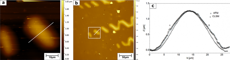
Using the elastic properties of EAu = 77 GPa and the Poisson’s ratio νAu = 0.44 of gold, the stresses calculated from the data of both imaging techniques with the Hutchinson and Suo model [31] are in good agreement. For example, when AFM measurements are used to calculate the critical buckling stress, the value is σb = 76 ± 24 MPa, compared to the CLSM where σb = 74 ± 23 MPa is determined. The Γ(Ψ) of the spontaneous buckles were calculated from the values measured by AFM and CLSM and are Γ(Ψ) = 0.7 ± 0.3 Jm-2 and Γ(Ψ) = 0.8 ± 0.3 Jm-2, respectively. The interfacial adhesion values are similar to that for the same interface measured with four-point bending (0.8 Jm-2). [3]
Because the compression-induced buckles were quite large, only CLSM was used to measure the buckle dimensions (Figure 4).
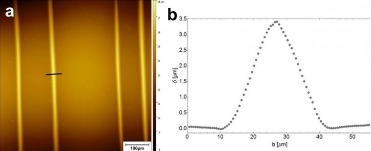
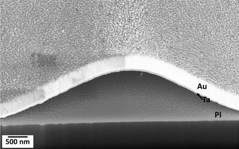
The buckle heights are almost three times larger than the spontaneously formed buckles of Au–PI. FIB cross-sectioning was used to determine that the Ta–PI interface fails (Figure 5). The critical buckling stress was calculated by Equation 1 to be approximately 350 MPa.
Using Equations 1 – 3 and the elastic properties of Au, the adhesion energy of the Au– Ta films on PI were determined to be Γ(Ψ) = ± 2.2 Jm-2, which is much higher than the Au film on PI without the Ta interlayer.
Conclusions
Au–PI film system with and without a Ta interlayer was examined using spontaneously produced buckles and compression-induced buckling. Incremental tensile straining was used to induce buckling of the Au–Ta films on PI. After 6% – 8% applied strain, buckles perpendic ular to the straining direction formed during unloading. In situ optical microscopy revealed that after 6% – 8% applied strain, compressive stress significant enough to induce buckling develops due to the elongation of the Au film during straining. The film elongates because the Au film plastically deforms via uniform necking across the whole film. Necking occurs on account of the good adhesion between the film and substrate, which helps to suppress catastrophic failure. This uniform deformation is in contradiction to the original theory that when a film delaminates from the substrate and becomes freestanding, plastic deformation will localize only at freestanding buckled areas. The Ta interlayer's improved adhesion provides the Au–PI interface, and the formation of the buckles perpendicular to the straining direction were crucial factors necessary to determine how film deformation and delamination are connected. With this new understanding, the lifetime and reliability of flexible electronics can be extended.
References
[1] A. C. Siegel, S. T. Phillips, M. D. Dickey, N. Lu, Z. Suo, G. M. Whitesides, Adv. Funct. Mater. 2010, 20, 28.
[2] J. A. Rogers, Z. Bao, K. Baldwin, A. Dodabalapur, B. Crone, V. R. Raju, V. Kuck, H. Katz, K. Amundson, J. Ewing, P. Drzaic, Proc. Natl. Acad. Sci. U. S. A. 2001, 98, 4835.
[3] J. D. Yeager, D. J. Phillips, D. M. Rector, D. F. Bahr, J. Neurosci. Methods 2008, 173, 279.
[4] B. A. Hollenberg, C. D. Richards, R. Richards, D. F. Bahr, D. M. Rector, J. Neurosci. Methods 2006, 153, 147.
[5] D. C. Agrawal, R. Raj, Acta Metall. 1989, 37, 1265.
[6] G. Rochat, Y. Leterrier, P. Fayet, J. Manson, Thin Solid Films 2003, 437, 204.
[7] S. Olliges, P. A. Gruber, V. Auzelyte, Y. Ekinci, H. H. Solak, R. Spolenak, Acta Mater. 2007, 55, 5201.
[8] P. A. Gruber, E. Arzt, R. Spolenak, J. Mater. Res. 2009, 24, 1906.
[9] O. Glushko, M. J. Cordill, Exp. Tech. 2014, 40, 303.
[10] W. P. Vellinga, J. T. M. de Hosson, P. C. P. Bouten, J. Appl. Phys. 2011, 110, 7.
[11] Q. Guan, J. Laven, P. C. P. Bouten, G. de With, Thin Solid Films 2016, 611, 107.
[12] O. Glushko, M. J. Cordill, A. Klug, E. J. W. List-Kratochvil, Microelectron. Reliab. 2016, 56, 109.
[13] G. D. Sim, Y. Hwangbo, H. H. Kim, S. B. Lee, J. J. Vlassak, Scr. Mater. 2012, 66, 915.
[14] K. L. Mittal, Electrocompon. Sci. Technol. 1976, 3, 21.
[15] A. A. Volinsky, N. R. Moody, W. W. Gerberich, Acta Mater. 2002, 50, 441.
[16] M. Lane, R. H. Dauskardt, A. Vainchtein, H. Gao, J. Mater. Res. 2000, 15, 2758.
[17] D. B. Marshall, A. G. Evans, J. Appl. Phys. 1984, 56, 2632.
[18] A. Bagchi, A. G. Evans, Thin Solid Films 1996, 286, 203.
[19] M. J. Cordill, D. F. Bahr, N. R. Moody, W. W. Gerberich, IEEE Trans. Device Mater. Reliab. 2004, 4, 163.
[20] M. J. Cordill, F. D. Fischer, F. G. Rammerstorfer, G. Dehm, Acta Mater. 2010, 58, 5520.
[21] J. Andersons, S. Tarasovs, Y. Leterrier, Thin Solid Films 2009, 517, 2007.
[22] G. Parry, C. Coupeau, J. Colin, A. Cimetière, J. Grilhé, Acta Mater. 2004, 52, 3959.
[23] G. Parry, J. Colin, C. Coupeau, F. Foucher, A. Cimetiere, J. Grilhe, Acta Mater. 2005, 53, 441.
[24] M. J. Cordill, A. A. Taylor, Thin Solid Films 2015, 589, 209.
[25] A. A. Taylor, M. J. Cordill, L. Bowles, J. Schalko, G. Dehm, Thin Solid Films 2013, 531, 354.
[26] V. M. Marx, C. Kirchlechner, I. Zizak, M. J. Cordill, G. Dehm, Philos. Mag. 2015, 95, 1982.
[27] B. Putz, R. L. Schoeppner, O. Glushko, D. F. Bahr, M. J. Cordill, Scr. Mater. 2015, 102, 23.
[28] M. J. Cordill, V. M. Marx, C. Kirchlechner, Thin Solid Films 2014, 571, 302.
[29] M. J. Cordill, O. Glushko, B. Putz, Front. Mater. 2016, 3, 1.
[30] S. Frank, U. A. Handge, S. Olliges, R. Spolenak, Acta Mater. 2009, 57, 1442.
[31] J. W. Hutchinson, Z. Suo, Adv. Appl. Mech. 1992, 29, 63.
[32] F. Cleymand, C. Coupeau, J. Colin, J. Grilhé, Eur. Phys. J. Appl. Phys. 2000, 10, 3.
[33] P. O. Renault, P. Villain, C. Coupeau, P. Goudeau, K. F. Badawi, Thin Solid Films 2003, 424, 267.
[34] J. D. Yeager, D. F. Bahr, Thin Solid Films 2010, 518, 5896.
[35] D. Nečas, P. Klapetek, Open Phys. 2012, 10, 181.
[36] F. Toth, F. G. Rammerstorfer, M. J. Cordill, F. D. Fischer, Acta Mater. 2013, 61, 2425.
[37] M. J. Cordill, D. F. Bahr, N. R. Moody, W. W. Gerberich, Mater. Sci. Eng. A 2007, 443, 150.
[38] J.-Y. Faou, G. Parry, S. Grachev, E. Barthel, Phys. Rev. Lett. 2012, 108, 1.
Copyright
DOI: 10.1002/adem.201600665; Andreas Kleinbichler, Mattias Bartosik, Bernhard Völker, and Megan J. Cordill
Advanced Engineering Materials; © 2016 WILEY-VCH Verlag GmbH & Co. KGaA, Weinheim
Source: Preview Image: jxfzsy/Getty Images