A Novel Slicing Method for Thin Supercapacitors
Thin and flexible supercapacitors with low cost and uniform thicknesses were fabricated by a new and efficient slicing method. The morphology of the thin supercapacitors was analyzed by scanning electron microscopy and laser scanning confocal microscopy, which revealed uniform thicknesses and well-formed interfaces between the electrode and the gel electrolyte. Tunable output voltages and energies were realized with a maximum specific capacitance of 248.8 F g-1 or
150.8 F cm-3. The devices showed a maintained 96% of the maximum specific capacitance after 300 cycles, and 91% specific capacitance retention when bent to a maximum angle of 180°.
Introduction
In recent years flexible and miniature electronic devices have accelerated the development of new energy storage systems.[1] Thin energy storage devices have shown promise in a variety of applications, including miniature robotics, implanted microelectronics, and wearable electronics.[1–12] Several strategies, such as photolithography, sputtering, laser scribing, and chemical vapor deposition, have been investigated for the fabrication of miniature electronics.[13–26] Despite the recent achievements, it remains challenging to realize uniform, neat, and low-cost fabrication of thin energy storage devices.
A slicing technique, which uses a sharp blade to cut bulk materials into thin slices, presents a general and efficient method that has been adopted in various fields. In biological and medical sciences, ultrathin slices of tissues and organs are obtained using a microtome. [27,28] Slicing offers low cost, controllable thickness, and small individual variation. However, it is rare to use slicing for microelectronic devices as there remain several challenges, including the difficulty in selecting suitable materials, instability for the interface between different components, and complexity in the design of device structure.
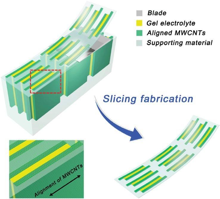
Herein, a new slicing method is developed for fabricating thin supercapacitors with low cost and individual variation. The fabrication of the thin supercapacitor is illustrated in Figure 1. Briefly, aligned multiwalled carbon nanotube (MWCNT) arrays with or without polyaniline (PANI) as electrodes and poly(vinyl alcohol) (PVA)/H3PO4 as the gel electrolyte.
The aligned MWCNT electrodes allow electrons to hop from one MWCNT to the neighboring others based on a 3D hopping mechanism.[29,30] The composites are embedded in epoxy resin, followed by cutting, using a microtome, into thin supercapacitors that are composed of many supercapacitor units. The thin supercapacitors are tunable in thickness, demonstrate uniform surfaces, and have compact interfaces for excellent electrochemical properties, e.g., a high specific capacitance of 248.8 F g-1 (150.8 F cm-3). This slicing method can be generally applied to the fabrication of other thin energy and electronic devices.
Methods
Aligned MWCNT arrays with an average height of 1 mm were vertically grown on silicon wafers via chemical vapor deposition. These arrays were uniaxially pressed with a precleaned glass slide and then removed from the substrate with a sharp blade.[31,32] To prepare the aligned MWCNT/PANI composites, the MWCNT film was immersed in an aqueous electrolyte containing 0.1 M aniline and 1 M sulfuric acid and polymerized electrochemically at a potential of 0.75 V using platinum wire counter electrode (CHI115, a diameter of 0.5 mm (0.02 in.)) and a silver/silver chloride (Ag/AgCl)l reference electrode (CHI111, a diameter of 4 mm).[33] The weight percentage of PANI was 70%, which was controlled by assuming an average of 2.5 electrons per aniline monomer. The resulting composite film was twice washed with deionized water and dried in the air before use.
The supercapacitors were fabricated by coating the MWCNT electrodes with PVA/ phosphoric acid (H3PO4)and treating in vacuo for 10 min to enhance the infiltration of the electrolyte into the electrodes. The above process was repeated at least two times. Next, the two electrodes were stacked together along the MWCNT-aligned direction to form a thin film supercapacitor. Each electrode shared a width of approximately 110 μm, and the distances between two electrodes ranged from 400 μm – 600 μm.
The stacked films were successively immersed in embedding solutions in acetone. The embedding solution was prepared by mixing an epoxy resin (SPI-PON 812) with T-168 (Shenyang Southeast Chemical Institute) as a plasticizer, dodecenyl succinic anhydride and methyl-5-norbornene-2,3-dicarboxylic anhydride (SPI Supplies Division of Structure Probe, Inc.) as curing agents, and 2,4,6-tris (dimethylaminomethyl phenol) (SPI Supplies Division of Structure Probe, Inc.) as a curing catalyst. Then the composite was put under vacuum to remove air bubbles.[34] It was then placed in a ribbon-shaped mold containing an embedding solution and cured at 60 °C (140 °F) for 24 h. The resulting sample was removed from the mold and fixed on the microtome sample stage. A tungsten carbide disposable blade (Leica TC65, a length of 65 mm, or 2.56 in.) was used to cut the thin supercapacitors along the direction of the aligned MWCNTs.
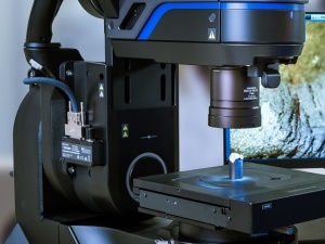
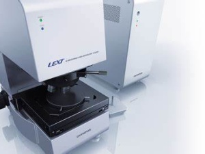
The structures were characterized by an Olympus LEXT OLS4100 laser scanning confocal microscope and scanning electron microscopy (Hitachi FE-SEM S-4800 operated at 1 kV). The thicknesses were measured using a stylus profilometer (Veeco Dektak 150). The electrical resistances were measured using a Keithley 2400 Source Meter. Electrochemical measurements and depositions were performed using an electrochemical workstation (CHI 660E). The cyclic stability was characterized by Arbin electrochemical cycler (MSTAT-5 V/10 mA/16 Ch).
Results
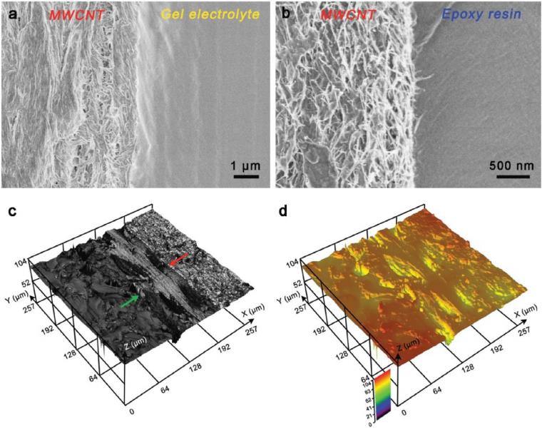
The slicing method enabled a controllable tuning of the device thickness from 10 μm – 60 μm. The gel electrolyte was in close contact with the aligned MWNCTs (Figure 2a). Close contact between the electrode and epoxy resin was also verified (Figure 2b), which is vital for the device to bend without breaking.
Furthermore, the 3D surface topography of the thin supercapacitor was characterized by laser scanning confocal microscopy. Figure 2c shows the reflection mode micrograph from laser scanning confocal microscopy. The green arrow indicates the interface between the MWCNT electrode and the gel electrolyte, and the red arrow indicates the interface between the electrode and the epoxy resin. Laser scanning confocal microscopy shows that the interfaces in the device are well-formed and relatively defect-free. Figure 2d shows the height map obtained from laser scanning confocal microscopy. The results show a uniform thickness without apparent defects at the interfaces, which is essential for high-performance electronic devices. The uniform surface and compact interfaces are attributed to the high compatibility of the constituent components.
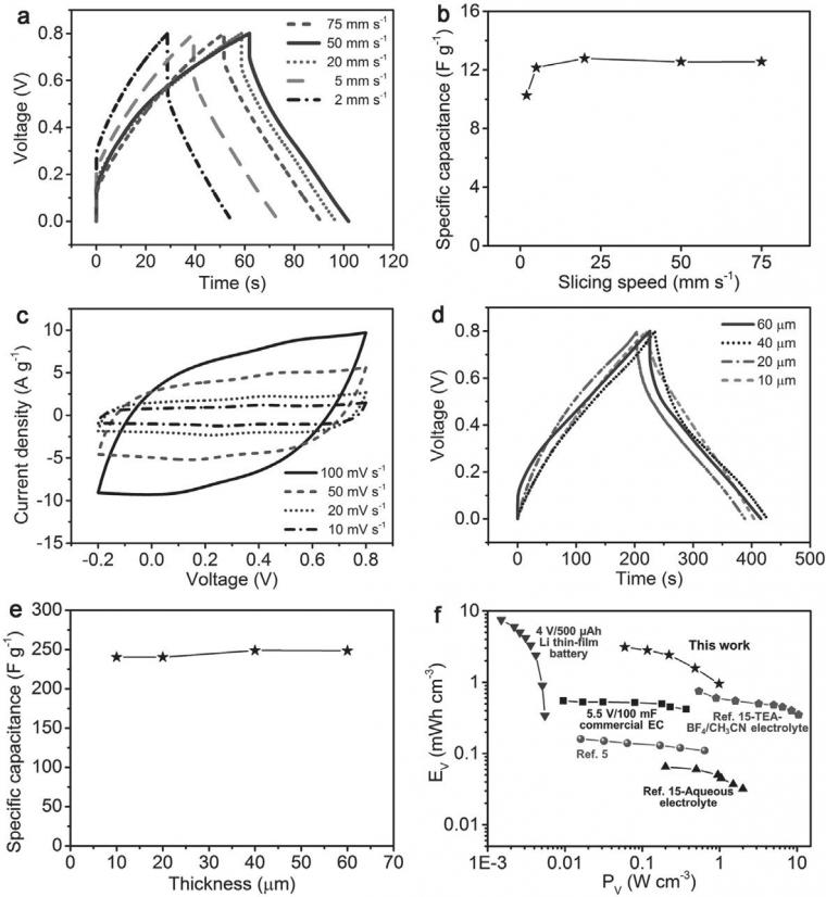
The dependence of the specific capacitance on slicing speed was investigated (Figure 3a). The specific capacitances of thin supercapacitors based on bare MWCNTs were increased from 10.3 F g-1 to 12.8 F g-1 with increasing slicing speed from 2 mm s-1 – 20 mm s-1 and remained almost unchanged from 20 mm s-1 – 75 mm s-1 (Figure 3b). This observation may be attributed to the relaxation of polymer chains in the gel electrolyte, which affects the interface with the MWCNTs at different slicing speeds. The relaxation of polymer chains is limited at higher slicing speeds; thus, a better interface between the MWCNT and gel electrolyte is formed, and the device has a lower internal resistance. This phenomenon was also verified by the decreasing internal resistance drop in the galvanostatic charge-discharge curves with increasing slicing speeds (Figure 3a). The specific capacitance reached a plateau at a slicing speed of 20 mm s-1. Therefore, a slicing speed of 20 mm s-1 was selected for further studies.
The introduction of PANI increased the specific capacitance of the supercapacitor. For the MWCNT/PANI composite electrodes, reversible charge-discharge performances at a variety of scan rates and current densities were achieved (Figure 3c), and a higher specific capacitance of 240 F g-1 (145.5 F cm-3) was achieved. The introduction of PANI increased the specific capacity by approximately 20 times compared to bare MWCNT electrodes. The performance enhancements were attributed to the high conductivity and rapid electron transport that arises from the incorporation of PANI in the porous MWCNT network, the pseudocapacitance associated with the uniformly coated PANI on the surfaces of MWCNTs, and the stable interfaces between the different components to retain high specific capacities after slicing.
For the MWCNT/PANI composites, with the increasing thickness from 10 μm – 60 μm, the galvanostatic charge-discharge was compared at a current density of 0.50 A g-1 (Figure 3d). The specific capacitances remained almost unchanged, with a maximum value, at 40 μm, of 248.8 F g-1 (150.8 F cm-3) (Figure 3e). The cyclic stability of the thin supercapacitor was verified by cyclic charge-discharge characterization, and the specific capacitance maintained by 96.0% of the maximum value after 2000 cycles. The energy and power densities reached 3.10 mW h cm-3 and 0.99 W cm-3, respectively, which are comparable to the previous reports on miniature energy storage devices and commercial counterparts (Figure 3f).[4,5,15,22].
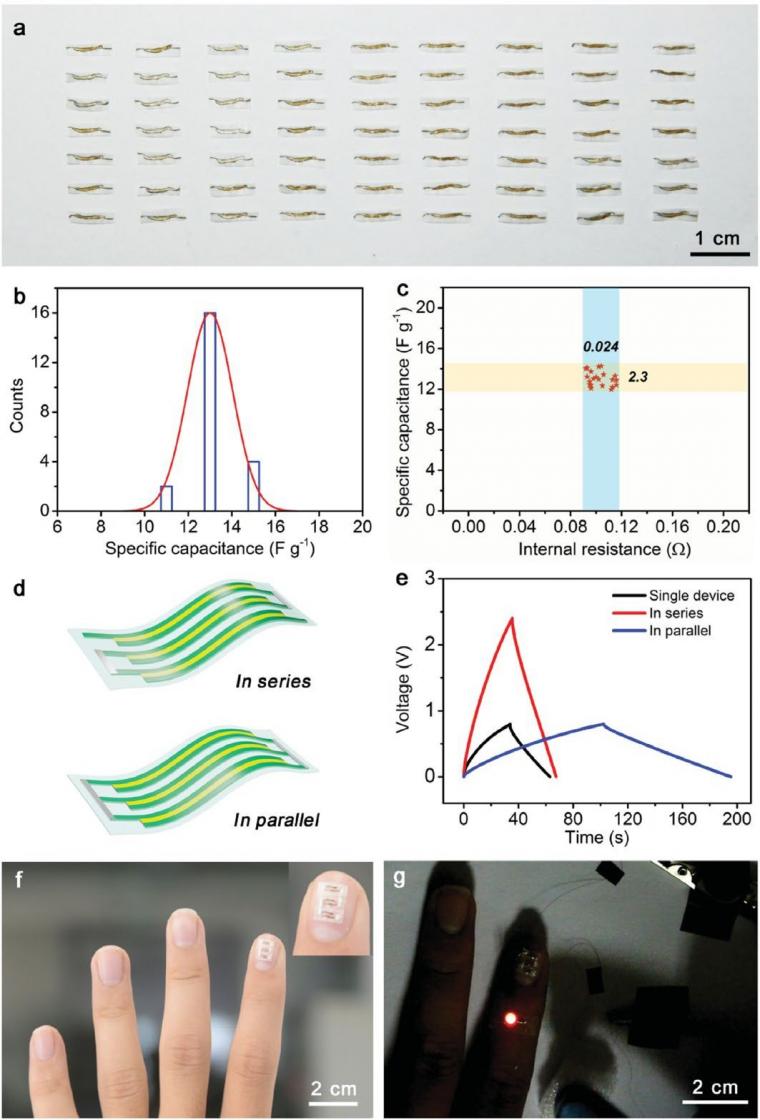
The slicing method shows several unique features that are favorable for practical applications. First, the individual variation of the obtained thin supercapacitors was small. For 22 thin supercapacitors produced under the same conditions, the specific capacitance and internal resistance only varied by 8.8% and 11.6%, respectively (Figure 4a–c). Second, the thin supercapacitors exhibit a low areal density, which is comparable to the state-of-theart thin energy storage devices and is promising for lightweight electronic devices.[24] Third, they have high flexibility, which is favorable for flexible electronics. The specific capacitance maintained 91% of its maximum value with increasing bending angles from 0° – 180°.
It recovered 96% of the specific capacitance after bending at 90° for 300 cycles. The slicing method also enables tunable connectivity of the devices to tune the output voltage and energy. For example, a thin supercapacitor with three units can be connected in series or parallel (Figure 4d), and the output voltage and discharge time were accordingly increased by three times (Figure 4e). As a proof-of-concept lightweight, thin, and flexible power source, a supercapacitor with three serial units was fixed on a fingernail (Figure 4f) to light up a commercial LED (Figure 4g).
Conclusions
In conclusion, a general and effective slicing method has been developed for the fabrication of thin supercapacitors with low cost and uniform thicknesses. The thin supercapacitors exhibit uniform surfaces, well-formed interfaces, and well-controlled thicknesses. A high specific capacitance of 248.8 F g-1 (150.8 F cm-3) was achieved with tunable output voltage and energy. The thin supercapacitors are demonstrated to be lightweight, thin, and flexible power sources to power commercial electronics. This slicing method is also compatible with the fabrication of a variety of other devices including, sensors, transistors, solar cells, and batteries for largescale production and high performances.
References
This text is a digest version of:
Sun, H., Fu, X., Xie, S., Jiang, Y., Guan, G., Wang, B., Li, H. and Peng, H. (2016), A Novel Slicing Method for Thin Supercapacitors. Adv. Mater., 28: 6429-6435. doi:10.1002/adma.201600506
[1] M. Beidaghi, Y. Gogotsi, Energy Environ Sci. 2014, 7, 867.
[2] J. Chmiola, C. Largeot, P. Taberna, P. Simon, Y. Gogotsi, Science 2010, 328, 480.
[3] D. Yu, K. Goh, Q. Zhang, L. Wei, H. Wang, W. Jiang, Y. Chen, Adv. Mater. 2014, 26, 6790.
[4] J. Ren, L. Li, C. Chen, X. Chen, Z. Cai, L. Qiu, Y. Wang, X. Zhu, H. Peng, Adv. Mater. 2013, 25, 1155.
[5] H. Sun, X. You, J. Deng, X. Chen, Z. Yang, J. Ren, H. Peng, Adv. Mater. 2014, 26, 2868.
[6] X. Dong, Z. Guo, Y. Song, M. Hou, J. Wang, Y. Wang, Y. Xia, Adv. Funct. Mater. 2014, 24, 3405.
[7] D. Yu, K. Goh, H. Wang, L. Wei, W. Jiang, Q. Zhang, L. Dai, Y. Chen, Nat. Nanotechnol. 2014, 9, 555.
[8] D. Yu, S. Zhai, W. Jiang, K. Goh, L. Wei, X. Chen, R. Jiang, Y. Chen, Adv. Mater. 2015, 27, 4895.
[9] W. Jiang, S. Zhai, Q. Qian, Y. Yuan, H. E. Karahan, L. Wei, K. Goh, A. K. Ng, J. Wei, Y. Chen, Energy Environ. Sci. 2016. 9, 611.
[10] D. Yu, Q. Qian, L. Wei, W. Jiang, K. Goh, J. Wei, J. Zhang, Y. Chen, Chem. Soc. Rev. 2015, 44, 647.
[11] M. Yu, Y. Han, X. Cheng, L. Hu, Y. Zeng, M. Chen, F. Cheng, X. Lu, Y. Tong, Adv. Mater. 2015, 27, 3085.
[12] M. Yu, Y. Zhang, Y. Zeng, M. S. Balogun, K. Mai, Z. Zhang, X. Lu, Y. Tong, Adv. Mater. 2014, 26, 4724.
[13] W. Gao, N. Singh, L. Song, Z. Liu, A. L. M. Reddy, L. Ci, R. Vajtai, Q. Zhang, B. Wei, P. Ajayan, Nat. Nanotechnol. 2011, 6, 496.
[14] L. Cao, S. Yang, W. Gao, Z. Liu, Y. Gong, L. Ma, G. Shi, S. Lei, Y. Zhang, S. Zhang, R. Vajtai, P. Ajayan, Small 2013, 9, 2905.
[15] M. Kady, S. Veronica, D. Sergey, R. B. Kaner, Science 2012, 335, 1326.
[16] Q. Meng, H. Wu, Y. Meng, K. Xie, Z. Wei, Z. Guo, Adv. Mater. 2014, 26, 4100.
[17] K. Wang, W. Zou, B. Quan, A. Yu, H. Wu, P. Jiang, Z. Wei, Adv. Energy Mater. 2011, 1, 1068.
[18] Z. Wu, K. Parvez, X. Feng, K. Müllen, Nat. Commun. 2013, 4, 2487.
[19] Z. Wu, K. Parvez, A. Winter, V. H. Vieker, X. Liu, S. Han, A. Turchanin, X. Feng, K. Müllen, Adv. Mater. 2014, 26, 4552.
[20] D. Qi, Z. Liu, Y. Liu, W. Leow, B. Zhu, H. Yang, J. Yu, W. Wang, H. Wang, S. Yin, X. Chen, Adv. Mater. 2015, 27, 5559.
[21] Z. Niu, L. Zhang, L. Liu, B. Zhu, H. Dong, X. Chen, Adv. Mater. 2013, 25, 4035.
[22] S. Kim, H. Koo, A. Lee, P. Braun, Adv. Mater. 2014, 26, 5108.
[23] C. Meng, J. Maeng, S. John, P. Irazoqui, Adv. Energy Mater. 2014, 4, 1301269.
[24] Z. Su, C. Yang, B. Xie, Z. Lin, Z. Zhang, J. Liu, B. Li, F. Kang, C. P. Wong, Energy Environ. Sci. 2014, 7, 2652.
[25] M. Beidaghi, C. Wang, Adv. Funct. Mater. 2012, 22, 4501.
[26] M. Beidaghi, C. Wang, Electrochim. Acta 2011, 56, 9508.
[27] A. Igersheim, O. Cichocki, Rev. Palaeobot. Palynol. 1996, 92, 389.
[28] W. Han, S. Heo, T. Driscoll, J. Delucca, C. McLeod, L. Smith, R. Duncan, R. Mauck, D. M. Elliott, Nat. Mater. 2016, 15, 477 .
[29] T. Chen, S. Wang, Z. Yang, Q. Feng, X. Sun, L. Li, Z. S. Wang, H. Peng, Angew. Chem. Int. Ed. 2011, 50, 1815.
[30] H. Peng, M. Jain, D. E. Peterson, Y. Zhu, Q. Jia, Small 2008, 4, 1964.
[31] Z. Yang, L. Li, H. Lin, Y. Luo, R. He, L. Qiu, J. Ren, H. Peng, Chem. Phys. Lett. 2012, 549, 82.
[32] H. Sun, R. Che, X. You, Y. Jiang, Z. Yang, J. Deng, L. Qiu, H. Peng, Adv. Mater. 2014, 26, 8120.
[33] A. Yu, I. Roes, A. Davies, Z. Chen, Appl. Phys. Lett. 2010, 96, 253105.
[34] a) L. Li, Z. Yang, H. Gao, H. Zhang, J. Ren,
X. Sun, T. Chen, H. G. Kia, H. Peng, Adv. Mater. 2011, 23, 3730 ; b) S. Huang, L. Li, Z. Yang,
L. Zhang, H. Saiyin, T. Chen, H. Peng, Adv. Mater. 2011, 23, 4707.
Copyright
H. Sun, X. Fu, S. Xie, Y. Jiang et al.; Advanced Engineering Materials; DOI: 10.1002/adma.201600506
© 2016 WILEY-VCH Verlag GmbH & Co. KGaA, Weinheim
Source: Preview Image: Grispb stock.adobe.com