Channel-Length Independent Electrical Characteristics of Oxide Thin-Film Transistors
Adapted from [1]
Introduction
Multi-component metal oxide thin film transistors (TFTs) including InGaZnO (IGZO) have gained popularity as a replacement for conventional Si-based TFTs due to their superior electrical properties, transparency, and large-area applicability. However, a gap still exists between emerging oxide and conventional Si-based TFTs in terms of field effect mobility (μFE), stability, and process immunity, which limit the widespread commercialization of oxide TFTs. To expand oxide TFT technology for broader applications, there is a high demand for short-channel capability, which can boost the driving current, increase integration density, reduce the dead area, and enhance productivity, among others. Besides, it is necessary to enable low leakage current in the scaled device.
To retain the advantages of a low leakage current in the short channel, careful control of the threshold voltage (Vth) is necessary, and operation in the enhancement mode is preferred. However, the well-known short-channel effects such as "hot carrier", drain-induced barrier lowering (DIBL), and reduced channel resistance can cause inconsistent electrical characteristics as the channel length (LCH) is shortened. Typically, oxide TFTs reported to date have LCH values of a few μm, limited by the photolithography process in large-area fabrication. It is common for Vth to shift negatively as LCH decreases, particularly for LCH values below 5 μm. This behavior reflects not only the above short-channel effects, but also defects attributable to impurities. This undesired behavior can be attributed to the lateral diffusion of carriers and impurities during the device integration process, which leads to the shortening of the effective channel length. Since the diffusion length is around a few micrometers, it is easy to attain the negative shift of Vth for TFTs with LCH shorter than 5 μm.
Herein, we propose a commercially favorable method using conventional SiOx to improve the back interface of IGZO TFTs and the short-channel capabilities.
Results
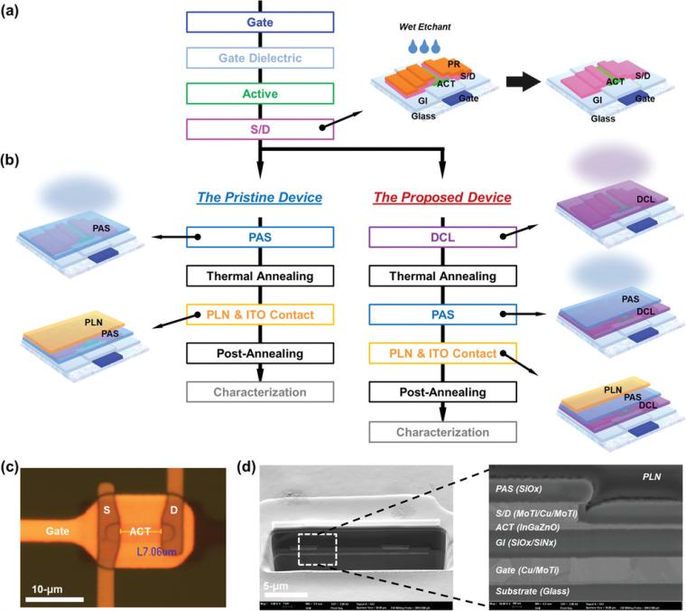
We used a conventional, inverted staggered structure with an etched back channel; full photolithography was conducted for fabrication. The top contact (Cu) served as the source/drain (S/D) electrode, defined by chemical wet etching (Fig. 1a). We fabricated two types of devices after the formation of S/D, the split layers are highlighted in Figure 1b. Equivalent processing variables such as precursor, gas flow rate, power, pressure, and temperature were applied during the formation of the defect control layer (DCL) and passivation (PAS) layer. The fabricated TFTs had a length (L) of 7 μm and a width (W) of 4 μm (Fig. 1c). Figure 1d presents a cross-sectional view of the pristine device.
To optimize the SiOx double-layer, we varied temperature, pressure, thickness, and annealing time while maintaining a total thickness of 200 nm for W/L = 4/7 μm to ensure desired switching behavior. To mitigate the impact of a thinner DCL on Vth (which becomes positive when DCL thickness is <80 nm), we used a 50 nm-thick DCL. The proposed device allowed for additional thermal treatments due to the sequential deposition process. Four cases were examined (no anneal, once at DCL, once at PAS, twice at PAS and DCL), revealing that annealing at the DCL improved Vth uniformity, while degradation was observed when annealing was performed at the PAS layer. This suggests that annealing at PAS may not effectively alleviate damage to the back channel due to impurities and/or defects. Therefore, annealing was only performed after DCL placement to achieve a positive Vth and good uniformity.
We examined the transfer characteristics of the proposed device as a function of the SiOx formation method, i.e. after wet etched, pristine device, and proposed device. Initially, the Vth was extremely negative after S/D patterning, and switching behavior was not observed. However, subsequent dielectric formation enabled switching characteristics. Remarkably, the effect of the DCL on device-to-device uniformity was evident, as devices with nine TFTs showed negligible leakage current under negative gate-to-source voltage (VGS) and uniform Vth distribution. The sequential formation of SiOx with appropriate thermal annealing in the proposed device resulted in increased and uniform Vth, indicating effective repair of backchannel damage and improved device stability. The increased Vth and improved subthreshold gate swing (S.S.) of the proposed device suggest reduced oxygen deficiency and carrier/defect generation. The average S.S. values of the pristine and proposed devices were 0.53 and 0.46 V dec−1, respectively. The larger trap density remaining in the pristine device compared to the proposed device, mainly due to the fabrication process of the SiOx layer formation upon the IGZO, contributed to the higher S.S. value in the pristine device.
Both the LCH-Dependent Vth range and the short-channel capability were drastically enhanced in the proposed device. A substantial difference emerged when LCH What < 7 μm. In the pristine device, the Vth became increasingly negative as the LCH became shorter and was extremely negative (<−5 V) at an LCH of 5 μm. Finally, all switching was lost at an LCH of 4 μm. In contrast, the Vth of the proposed device always had a positive value, and even the device with an LCH of 4 μm maintained appropriate switching.
The transfer characteristics facilitate simple DIBL quantification; the change in Vth is divided by the applied drain bias difference (VDS = 0.1, 10 V) [2,3]. Notably, this falls substantially from 177 in the pristine device to 84 mV V−1 in the proposed device, at an LCH of 5 μm. Because only appropriate switching characteristics at LCH < 5 μm were observed in the proposed device, the actual difference becomes more serious at shorter LCH. Thus, the proposed device is less sensitive than the pristine device to drain bias, even at LCH <5 μm.
Throughout the conduction path, the total equivalent resistance of a transistor is composed of channel resistance (RCH) and parasitic resistance (R0) (series and contact resistances). As the LCH decreases, the RCH decreases and the remaining R0 is the limiting factor in terms of short-channel device capability [4]. Thus, it appears that the total equivalent resistance and the effective channel of the proposed device are different from that of the pristine device. Besides, both devices commonly exhibited increased μFE as decreasing LCH. The proposed method for forming the device with DCL appears to influence the channel configuration. Furthermore, in a short-channel device, the portion of LCH that makes the greatest contribution to the gate bias dependency should be considered when estimating device mobility [5]. Thus, it is better to compare effective length-based mobilities (μFE _Leff) that consider the effective channel length (Leff).
To validate our assumptions and clarify the detailed geometry of LCH, we conducted calculations of total resistance using the transmission line method (TLM). The results showed that the region of conducting behavior in the pristine device was sufficiently long, indicating high conductivity below 4 μm. In contrast, the region of conducting behavior in the proposed device was shorter, at ≈2.9 μm, and the resistance (R0) was slightly increased. This reduced region of conducting behavior suggests a longer Leff in the proposed device, with a larger proportion of Leff within the LCH, allowing for switching despite the shorter channel length (4 μm). The results showed that the proposed method with DCL mainly affects Vth rather than device mobility as the LCH decreases.
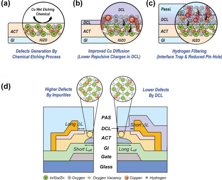
From transmission electron microscopy and energy-dispersive X-ray spectroscopy, we have found that the DCL supplies oxygen to the oxygen-deficient back channel, filters inter-diffused hydrogen, and boosts out-diffusion of residual Cun+ from the back channel (Fig. 2a–c). Although these crucial functions were partly provided by the pristine PAS as a single layer, they were greatly enhanced by our method as a double layer with DCL, affording stable electrical characteristics even in short channels. Our process-dependent investigations revealed how the damaged IGZO recovered. As IGZO defects were thus controlled, the backchannel properties noticeably improved. Current flow in the back channel was confined, effectively redefining the channel (Fig. 2d).
Conclusion
We proposed a fabrication method to address Vth non-uniformity in downscaled devices. By sequentially forming a double-layered dielectric of homogeneous SiOx at the back channel, we achieved advanced functionality compared to conventional materials. The DCL greatly improved the electrical characteristics of back-channel wet-etched IGZO TFTs, enabling consistent Vth values as LCH decreased from 20 to 4 μm. The poor performance of short LCH devices, caused by back-channel defects from wet etching and SiOx deposition, was effectively recovered by the DCL. Additionally, the effective LCH was increased by reducing the region of conducting behavior, allowing for appropriate switching even at 4 μm LCH with superior performance. Furthermore, the proposed device exhibited a dramatically reduced Vth Range AS LCH varied from 20 to 4 μm, thanks to the multi-functional DCL.
References
[1] Kyung K.M. et al. (2023). Suppressing Undesired Channel Length-Dependent Electrical Characteristics of Fully Integrated InGaZnO Thin-Film Transistors via Defect Control Layer. Adv. Electron. Mater. DOI.10.1002/aelm.202200986
[2] Raja, J. et al. (2014). Drain-induced barrier lowering and parasitic resistance induced instabilities in short-channel InSnZnO TFTs. IEEE Electron Device Letters. DOI: 10.1109/LED.2014.2318754.
[3] Kim, S.C. et al. (2015). Short channel amorphous In–Ga–Zn–O thin-film transistor arrays for ultra-high definition active matrix liquid crystal displays: Electrical properties and stability. Solid-State Electronics. DOI: 10.1016/J.SSE.2015.05.002.
[4] Zhao, Y. et al. (2020). High Performance Indium-Gallium-Zinc Oxide Thin Film Transistor via Interface Engineering. Advanced Functional Materials. DOI: 10.1002/ADFM.202003285.
[5] Kim, H.W. et al. (2018). Influence of effective channel length in self-aligned coplanar amorphous-indium-gallium-zinc-oxide thin-film transistors with different annealing temperatures. Applied Physics Letters. DOI: 10.1063/1.5027373.
Source: Image: Kyung, K.M.