Multiscale and Uniform Liquid Metal Thin‐Film Patterning Based on Soft Lithography for 3D Heterogeneous Integrated Soft Microsystems: Additive Stamping and Subtractive Reverse Stamping
The use of intrinsically soft conductors, such as liquid eutectic gallium–indium alloy (EGaIn), has enabled the fabrication of bioinspired soft electronics. The fabrication of EGaIn thin films with high resolution and size scalability is one of the primary technical hurdles. Soft lithography using wetting/nonwetting surface modifications and 3D heterogeneous integration can address these challenges. This study demonstrates multiscale EGaIn thin-film patterning by utilizing additive stamping for large-scale (mm–cm) soft electronics and subtractive reverse stamping for microscale (μm–mm) soft electronics. These structures can be integrated to fabricate several functional soft microsystems.
Abstract
The use of intrinsically soft conductors, such as liquid eutectic gallium–indium alloy (EGaIn), has enabled the fabrication of bioinspired soft electronics. The fabrication of EGaIn thin films with high resolution and size scalability is one of the primary technical hurdles. Soft lithography using wetting/nonwetting surface modifications and 3D heterogeneous integration can address these challenges. This study demonstrates multiscale EGaIn thin-film patterning by utilizing additive stamping for large-scale (mm–cm) soft electronics and subtractive reverse stamping for microscale (μm–mm) soft electronics. These structures can be integrated to fabricate several functional soft microsystems.
Introduction
Bioinspired soft functional material synthesis [1,2] and manufacturing technology [3,4] for soft electronics has applications ranging from entertainment to healthcare. [5,6] Unlike conventional solid-state electronics, soft electronics are lightweight, stretchable, reconfigurable, and biocompatible for skin-mountable and wearable sensors. [7,8] Flexibility and stretchability are achieved by using either 3D solid metal patterns [9,10] or elastic polymer matrices with embedded conductive nanomaterials. [11,12]
An alternative approach to realize soft microsystems is to use intrinsically soft conductors, e.g., liquid eutectic gallium–indium alloy (EGaIn). EGaIn-based soft electronics are nontoxic, mechanically stable, and highly stretchable. Also, the low melting temperature (< 15 °C (59 °F)) and negligible vapor pressure facilitate room-temperature and ambient pressure manufacturing. [13–15] Moreover, thanks to the formation of a thin oxide layer on the EGaIn surface, [16,17] the formed structures maintain their mechanical shapes on a soft elastomeric substrate, such as poly(dimethylsiloxane) (PDMS).
A broad range of patterning methods based on lithography-enabled stamping and stencil printing, injection, as well as additive and subtractive direct write/patterning processes have been implemented for EGaIn microsystems. [18–24] Limitations of lithography-defined stencils are the relatively low resolution, rough EGaIn surface, and excessive EGaIn loss during the stencil lift-off process. Subtractive direct patterning techniques using laser ablation [25,26] or electrochemical reduction [27,28] enable an inexpensive and facile approach to pattern fine EGaIn lines, but the serial process makes EGaIn removal slow in the case of patterning small EGaIn features on large substrates. Further, manually spreading EGaIn using a roller results in rough surfaces with holes in the EGaIn film. [18] Direct write and injection techniques address this issue, [29–32] but the resolution is limited. Microfluidic injection [33,34] and vacuum filling [35,36] provide high resolution, but the microchannels require relatively large thicknesses. Using a microtransfer deposition process based on soft lithography, [37] EGaIn features > 2 μm can be achieved, but the technology suffers from residues formed outside of the channel areas.
Soft lithography offers a simple, fast, and low-cost way to pattern multiscale EGaIn films. However, the surface oxide layer on EGaIn interferes with uniform wetting on soft elastomeric substrates. Stamp lithography is often regarded as the lowest resolution and least reliable technique among the additive printing methods. [18,19,38] By utilizing chemical and physical surface modification of the elastomeric substrates, [39,40] the PDMS surfaces can be modified to have selective nonwetting or wetting properties. The nonwetting characteristics of chemically modified PDMS surfaces hinder the formation of EGaIn residue, while the uniform wetting characteristics of physically modified PDMS surfaces assist in the formation of thin and smooth films.
Recently, we demonstrated high resolution, uniform, and residue-free EGaIn patterning, ranging from single micrometer to millimeter scales, by utilizing a chemical surface modification and residue transfer process using a reverse stamping approach. [41]
Building on our previous work, [41–44] this study presents multiscale and uniform EGaIn thinfilm patterning by utilizing additive stamping for largescale (mm–cm) soft electronics and the subtractive reverse stamping for microscale (μm–mm) soft electronics. By combining these complementary patterning techniques using 3D heterogeneous integration, fabricated and optimized soft electronic components built with different patterning processes can be integrated to form high-density and multifunctional soft microsystems.
Methods
Figure 1 illustrates the complementary multiscale EGaIn thin-film patterning processes based on soft lithography. The underlying liquid metal patterning processes mainly consist of three steps: 1) microtransfer molding of EGaIn, 2) EGaIn transfer using subtractive reverse stamping or additive stamping, and 3) sealing and interconnection. Chemical surface modification of the PDMS mold (for the subtractive approach) or the PDMS stamp (for the additive approach) using toluene is performed to increase the hydrophobicity. The PDMS mold/stamp is then coated by pressing onto a donor PDMS substrate coated with EGaIn.
For the subtractive approach (Figure 1a), the PDMS stamp is reverse stamped to remove EGaIn residue on the protruding surfaces to a sacrificial PDMS layer. The reverse stamping process yields fine, uniform, and thin EGaIn lines inside of the PDMS channels without residues on the surrounding protruding surfaces. Information). The subtractive approach showed size scalability from 2 μm to 1 mm – 2 mm in line width. [41]
For the additive stamping approach, a PDMS stamp wet with EGaIn is stamped onto a paper-textured PDMS substrate (Figure 1b).
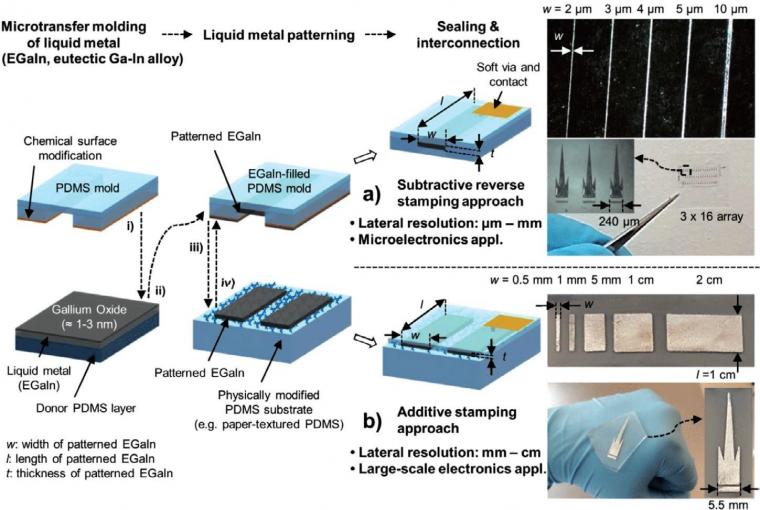
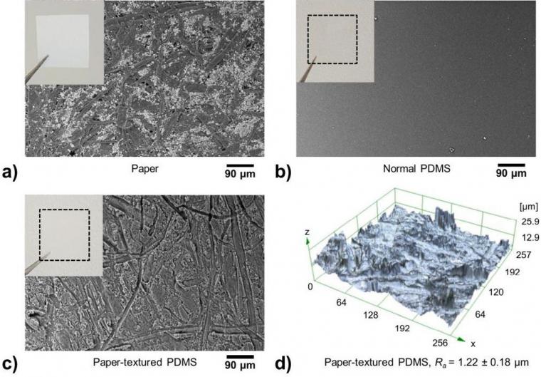
The paper texture, comprised of randomly distributed micro cellulose fibers (Figure 2a), is transferred to a PDMS surface using a conventional PDMS casting method. The resulting paper-texture PDMS exhibits a surface microstructure which allows it to be wet by EGaIn (Figure 2b–d). As a result, continuous EGaIn films can be transferred to paper-textured PDMS with multiple stamping steps.
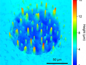
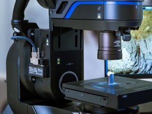
Surface characterizations were performed using an Olympus LEXT OLS4000 3D laser scanning confocal microscope and scanning electron microscopy (SEM, Hitachi S-3700N Variable Pressure SEM). Electrical characterizations of the soft, passive components, circuits, and LC resonator were performed using a multimeter (Hewlett Packard 34401A), a source meter (Keithley 2636A), and an LCR meter (Agilent 4284A). For mechanical stretching and bending characterizations, a linear motion stage and circular glass cylinders (radius: 10 mm (0.4 in.)) were prepared, respectively. Thermal characterizations of the soft heater were performed using a source meter (Keithley 2636A) to supply power, and temperature increases were recorded using an IR camera (FLIR T640).
Results and Discussion
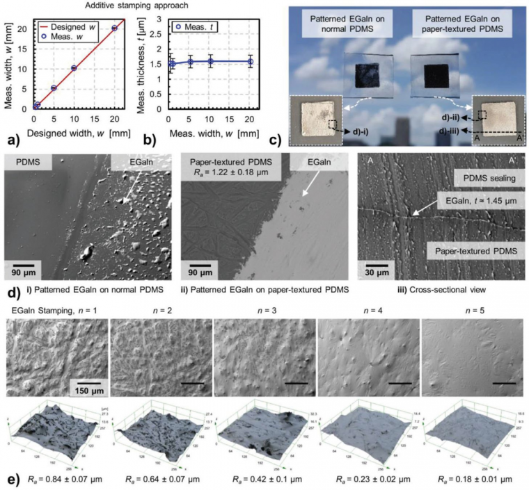
Figure 3a,b shows the measured EGaIn width as a function of the stamp width and the resulting film thickness as a function of the patterned EGaIn width, respectively. Figure 3c,d shows the non-uniform patterned EGaIn films deposited on a standard PDMS surface and a smooth uniform EGaIn film on paper-textured PDMS surface. PDMS stamps were stamped five times on paper-textured PDMS substrates to achieve smooth and uniform films. Figure 3e shows the SEM and 3D scanning laser confocal microscopy reflection mode images of stamped EGaIn, showing the evolution of the height variation with successive stamping. The additive stamping process decreases the surface roughness (Ra) with an increasing number of stamping steps, which indicates that the stamped EGaIn film is getting smoother. The random, micrometer-sized features, as characterized by scanning confocal laser microscopy in reflection mode, on the paper-textured PDMS surface (Figure 2b) were partially wetted during the initial one to two stamping steps, ultimately filling the grooved areas with EGaIn. After stamping five times, the surface structures of the paper-textured PDMS were entirely covered with EGaIn, showing a uniform and smooth EGaIn thin film.
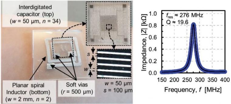
Using the additive stamping process, soft, passive components and circuits were fabricated, and their electrical and mechanical characteristics were investigated. Figure 4a shows a soft resistor, planar spiral inductor, and interdigitated capacitor, all having a 1 mm (0.04 in.) line width and 1 mm (0.04 in.) line spacing.
Figure 4b shows a simple circuit comprised of a 5 × 5 array of light-emitting diodes (LED).
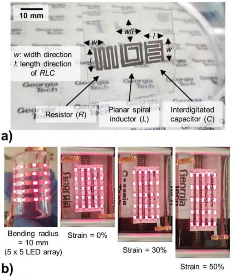
A constant current was applied to the LED array, which was subjected to bending (bending radius, r = 10 mm (0.4 in.)) and stretching (strain, e) deformation. The soft circuit withstood the bending and strain deformations (up to e = 50%) while maintaining its functionality.
By combining the proposed multiscale EGaIn thin-film patterning techniques via 3D heterogeneous integration, more complex soft microsystems were fabricated. Three different soft functional microsystems were fabricated:
i. a soft inductor-capacitor (LC) resonator,
ii. a fingertip-mountable, soft oximeter, and
iii. soft heaters with localized or distributed heating. Figure 5 shows the LC resonator. The interdigitated capacitor was fabricated using subtractive reverse stamping, and its areal capacitance was 13.2 pF cm-2, which is roughly nine times higher than what would be achievable with additive stamping. The planar coil inductor, as well as the readout coil, were fabricated using additive stamping. After 3D integration of the LC components using liquid-metal filled vias, the soft microsystem was wirelessly interrogated using a readout coil to collect the resonance frequency. The measured resonance frequency was 276 MHz, which also agreed well with the calculated value, and the Q factor was ≈20 (Figure 5b).
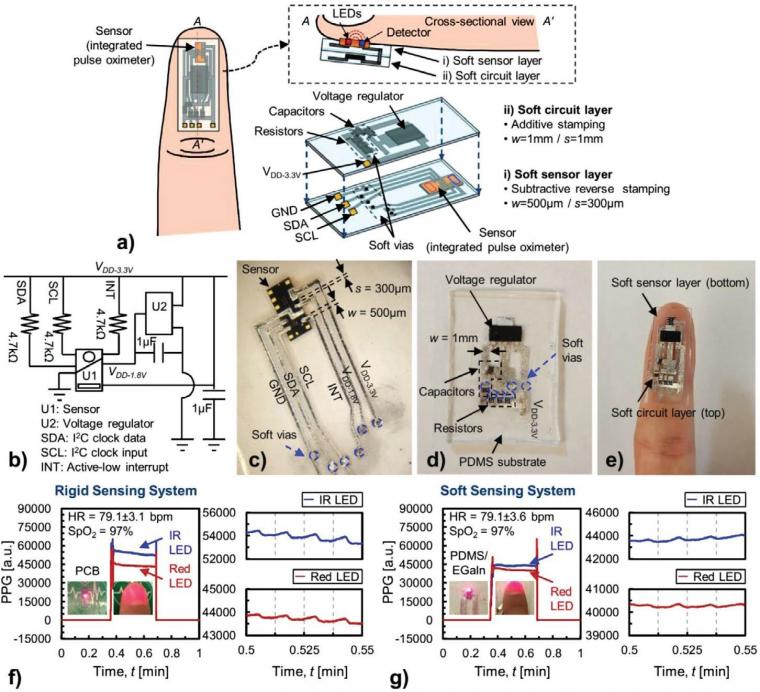
A fingertip-mountable, soft, and 3D-integrated biological sensor, comprised of a soft sensing layer with a commercial pulse oximeter and a soft interfacing circuit layer, is demonstrated for noninvasive and real-time heart rate (HR) and blood oxygen monitoring (Figure 6a). This soft sensor layer is fabricated using subtractive reverse stamping to connect the integrated pulse oximeter (MAX30100, Maxim Integrated Products Inc.), while additive stamping is utilized to fabricate the soft printed circuit board for the interfacing circuit (Figure 6b–d). These soft sensor and circuit layers are then vertically interconnected through soft vias (Figure 6e). The photoplethysmogram (PPG) waveforms using an IR LED and a red LED, and the extracted HR and saturation of peripheral oxygen (SpO2) using the PDMS/ EGaIn-based soft sensing system are shown in Figure 6f,g. The results were comparable to a rigid PCB-based sensing system.
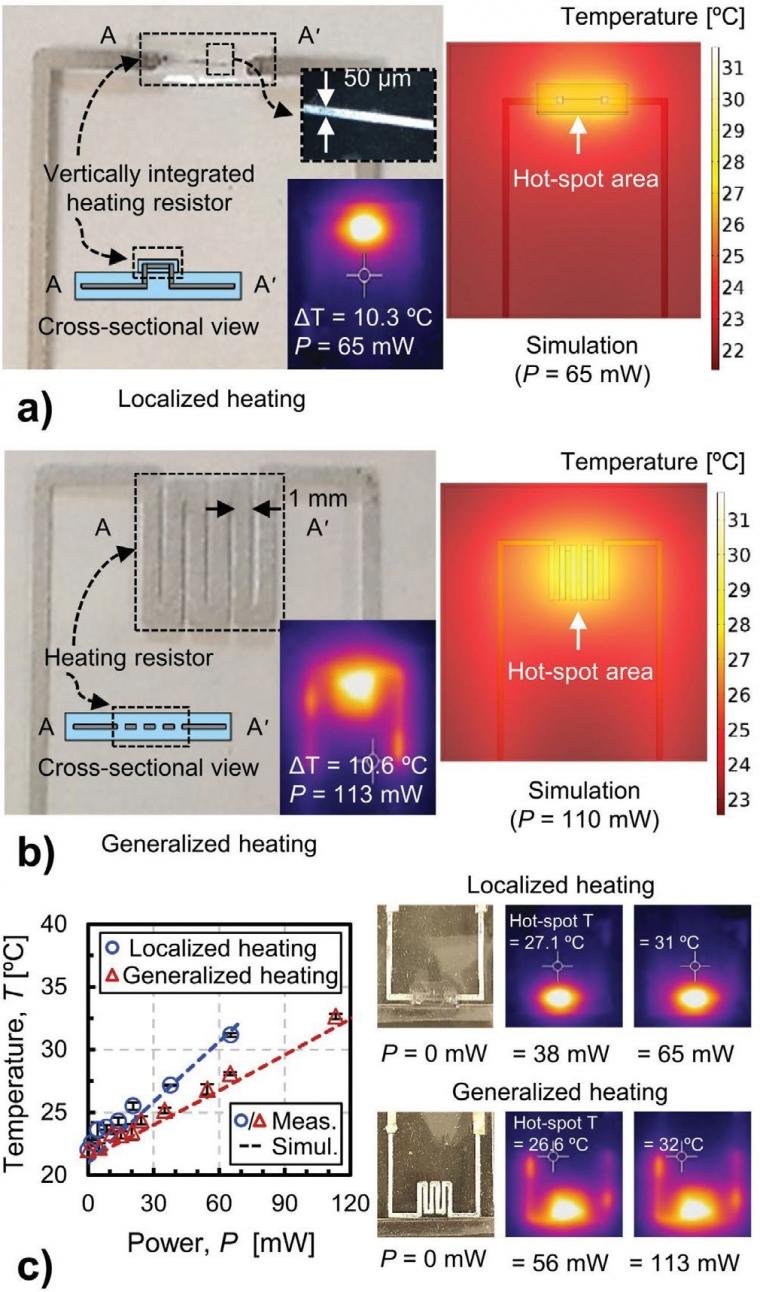
Finally, soft heaters based on EGaIn thinfilm resistors are demonstrated for localized and distributed heating applications. For the localized heating applications (Figure 7a), a 50 μm wide heating resistor fabricated using subtractive reverse stamping and was vertically integrated on a soft circuit. For large area heating applications (Figure 7b), a 1 mm (0.04 in.) wide serpentine heating resistor was fabricated using additive stamping. Figure 7c shows the measured and simulated hot-spot temperature as a function of the applied power. To reach a temperature increase of ΔT ≈ 10 °C (50 °F), the vertically integrated microheater requires 65 mW, while the serpentine-shaped heater heats a larger area but requires 113 mW. Compared to other heaters, [45–47] the fabricated soft heaters using thin-film resistors showed 8 times higher heating efficiency. In addition to efficient heating, the soft heater provides flexibility and stretchability for wearable and skin mountable electronics applications.
Conclusions
This study reports the multiscale and uniform, thin-film patterning of EGaIn using soft lithography by utilizing subtractive reverse stamping for high-density microscale patterns and additive stamping for centimeter-scale patterns. Considering the size scalability of the thin-film patterning and the possibility to heterogeneously integrate structures fabricated with either technique, soft electronic components can be fabricated and integrated to form soft and flexible multifunctional microelectronics.
References
This text is the digest version of the following article:
Advanced Materials Technologies
[1] A. Thomas, Angew. Chem., Int. Ed. 2010, 49, 8328.
[2] X. Chen, H. Fuchs, Soft Matter Nanotechnology, Wiley-VCH, Weinheim 2015.
[3] R. L. Truby, J. A. Lewis, Nature 2016, 540, 371.
[4] C. S. O’Bryan, T. Bhattacharjee,
S. R. Niemi, S. Balachandar, N. Baldwin,
S. T. Ellison, C. R. Taylor, W. G. Sawyer,
T. E. Angelini, MRS Bull. 2017, 42, 571.
[5] A. M. Hussain, M. M. Hussain, Adv. Mater. 2016, 28, 4219.
[6] A. Chortos, Z. Bao, Mater. Today 2014, 17, 321.
[7] J. A. Rogers, R. Ghaffari, D.-H. Kim, Stretchable Bioelectronics for Medical Device and Systems, Springer, Switzerland 2016.
[8] T. Someya, Stretchable Electronics, Wiley-VCH, Weinheim 2012.
[9] S. Xu, Y. Zhang, L. Jia, K. E. Mathewson, K.-I. Jang, J. Kim, H. Fu, X. Huang, P. Chava, R. Wang, S. Bhole, L. Wang, Y. J. Na, Y. Guan, M. Flavin, Z. Han, Y. Huang,
J. A. Rogers, Science 2014, 344, 70.
[10] S. Xu, Z. Yan, K.-I. Jang, W. Huang, H. Fu,
J. Kim, Z. Wei, M. Flavin, J. McCracken, R. Wang,
A. Badea, Y. Liu, D. Xiao, G. Zhou, J. Lee,
H. U. Chung, H. Cheng, W. Ren, A. Banks,
X. Li, U. Paik, R. G. Nuzzo, Y. Huang, Y. Zhang,
J. A. Rogers, Science 2015, 347, 154.
[11] K. Chen, W. Gao, S. Emaminejad,
D. Kiriya, H. Ota, H. Y. Y. Nyein, K. Takei, A. Javey, Adv. Mater. 2016, 28, 4397.
[12] M. Segev-Bar, H. Haick, ACS Nano 2013, 7, 8366.
[13] M. D. Dickey, R. C. Chiechi, R. J. Larsen,
E. A. Weiss, D. A. Weitz, G. M. Whitesides, Adv. Funct. Mater. 2008, 18, 1097.
[14] N. Kazem, T. Hellebrekers, C. Majidi, Adv. Mater. 2017, 29, 1605985.
[15] K. Khoshmanesh, S.-Y. Tang, J. Y. Zhu,
S. Schaefer, A. Mitchell, K. Kalantar-zadeh,
M. D. Dickey, Lab Chip 2017, 17, 974.
Source: Preview Image: Phawat/stock.adobe.com