Boosted UV Photodetection Performance in Chemically Etched Amorphous Gallium(III) Oxide Thin-Film Transistors
Bottom-gate amorphous gallium oxide (Ga2O3) (a-Ga2O3) thin-film transistors (TFTs) were fabricated to boost their UV photodetection properties. A simple chemical-etching solution was employed that is easy to use, low cost, and compatible with traditional lithographic processes to selectively etch a-Ga2O3 films. The a-Ga2O3 channel etched device, on silicon, effectively suppresses gate leakage current. Further, a patterned a-Ga2O3 TFT on quartz shows excellent n-type TFT performance with a high on/off ratio of approximately 107. It is also applied as a phototransistor, to diminish the persistent photoconductivity (PPC) effect while keeping a high responsivity (R). Under 254 nm UV illumination, the a-Ga2O3 phototransistor demonstrated a high light-to-dark ratio of 5 × 10⁷, a high responsivity of R = 5.67 × 10³ A W-1, and a high detectivity of 1.87 × 10¹⁵ Jones. The PPC phenomenon in a-Ga2O3 UV phototransistors was effectively suppressed by applying a positive gate pulse, which significantly shortens the decay time to 5 ms and enables possible imaging applications.
Abstract
Bottom-gate amorphous gallium oxide (Ga2O3) (a-Ga2O3) thin-film transistors (TFTs) were fabricated to boost their UV photodetection properties. A simple chemical-etching solution was employed that is easy to use, low cost, and compatible with traditional lithographic processes to selectively etch a-Ga2O3 films. The a-Ga2O3 channel etched device, on silicon, effectively suppresses gate leakage current. Further, a patterned a-Ga2O3 TFT on quartz shows excellent n-type TFT performance with a high on/off ratio of approximately 107. It is also applied as a phototransistor, to diminish the persistent photoconductivity (PPC) effect while keeping a high responsivity (R). Under 254 nm UV illumination, the a-Ga2O3 phototransistor demonstrated a high light-to-dark ratio of 5 × 10⁷, a high responsivity of R = 5.67 × 10³ A W-1, and a high detectivity of 1.87 × 10¹⁵ Jones. The PPC phenomenon in a-Ga2O3 UV phototransistors was effectively suppressed by applying a positive gate pulse, which significantly shortens the decay time to 5 ms and enables possible imaging applications.
Introduction
Amorphous galium oxide (Ga2O3) (a-Ga2O3) has attracted increasing attention for its wide range of applications in deep ultraviolet (UV) photodetection, such as confidential space communication, imaging, flame detection, and missile warning systems. [1–4] Two-terminal Ga2O3 photodetectors (PDs) are the most commonly investigated, but their slow response speed, caused by persistent photoconductivity (PPC), [5,6] impedes their further application. [7] PPC occurs in most oxide semiconductor materials because of the large quantity of oxygen vacancy (Vo) defects and the high density of trap states. [8,9]
Three-terminal PD, or phototransistors, have an additional terminal-gate to control the channel carriers’ transportation behavior are regarded as an alternative solution to improve the PD performance.[10,11] Phototransistors have the intrinsic gain of transistors and regular photoconductors, which makes it possible to achieve high light-to-dark current ratios and responsivity (R).[11,12] PPC can be eliminated by exerting a gate pulse, as demonstrated by Jeon et al. in a three-terminal photosensor array.[5] For a-Ga2O3 UV PD or imaging applications, research is needed to suppress PPC and raise the response speed while retaining a R. The controllable and selective etching of a-Ga2O3 channels to metals and other oxides is critical to achieving a low gate leakage current and favorable transfer characteristics. [13,14] Wet chemical etching of b-Ga2O3 has been demonstrated by using phosphoric acid (H3PO4) and sulfuric acid (H2SO4). [15,16] However, these strong acids readily corrode metals and oxides, which makes device fabrication difficult.
In this study, we present bottom-gate a-Ga2O3 thin-film transistors (TFTs) and phototransistors, where the a-Ga2O3 channels were selectively etched using tetramethylammonium hydroxide (TMAH) aqueous solution. This new etching method is low cost, simple, safe, and is compatible with conventional lithographic techniques. For the bottom-gate Ga2O3 TFT on silicon, the patterned channel device exhibits superior transistor characteristics compared to the unpatterned one. A bottom-gate a-Ga2O3 phototransistor with interdigitated source/ drain (S/D) electrodes was prepared on quartz and used to detect deep UV rays. It demonstrated typical transistor output and transfer characteristics with a high on/off ratio of approximately 107. Meanwhile, excellent photodetector performance was demonstrated under a 254 nm UV illumination, including a high light-to-dark ratio of 5 × 10⁷ and R = 5.67 × 10³ A W-1. By applying a positive gate pulse, PPC in the a-Ga2O3 phototransistors is effectively eliminated with a fast decay in 5 ms.
Methods
Common-gated a-Ga2O3 TFTs were fabricated on silicon dioxide (SiO2) (300 nm)/Si substrates. An a-Ga2O3 channel layer (25 nm) was deposited by RF-sputtering using a Ga2O3 ceramic target (99.999% pure) at room temperature and patterned by UV-lithography followed by wet chemical etching in a TMAH solution. The ITO (100 nm) S/D electrodes were prepared by UV-lithography and lift-off process, where the film deposition was carried out in a sputtering chamber. Bottom gate staggered a-Ga2O3 TFTs were fabricated was deposited by RF-magnetron sputtering and wet etched after the lithography to form the bottom gate electrode. Then, aluminum oxide (Al2O3) (110 nm) was grown on the gate metal at 200 °C (392 °F) in the ALD system and patterned by the combined process of UV-lithography and wet etching in an H3PO4 solution.
After that, a 25 nm a-Ga2O3 layer was sputtered, which is also patterned into discrete rectangles with dimensions of 175 μm × 600 μm. Next, interdigitated S/D electrodes are defined by UV-lithography. The S/D electrodes have 15 pairs of fingers with 10 μm in width, 10 μm in spacing gap, and 145 μm in length. At last, a sequential deposition of tin (Ti) and gold (Au) layers were deposited in the RF-magnetron sputtering system with a thickness of 20 nm and 80 nm, respectively, which are further patterned by the following lift-off process.
Film thickness was measured by a stylus profiler (KLA-Tencor P-6 Stylus Profiler). The surface morphology was evaluated by atomic force microscopy (AFM, Bruker Dimension EDGE), laser scanning confocal microscope (Olympus LEXT OLS5000 system), and scanning electron microscopy (SEM, Zeiss Sigma 300).
The electrical properties were analyzed using a Keithley 4200 and a Keithley 6487. A handheld UV 254 nm lamp (ZF-5) and a xenon lamp with Omni-l 180i grating spectrometer were used.
Results and Discussion
The etching behaviors of two a-Ga2O3 samples were first investigated using different TMAH concentrations and temperatures. The a-Ga2O3 films are labeled as S1 and S2, which are sputtered with oxygen (O2) and without O2 flux, respectively. Both of the samples are amorphous. S1 and S2 have different densities, determined from X-ray reflection spectra (XRR), which are 5.32 g cm-3 (332 lb ft-3) and 4.84 g cm-3 (302 lb ft-3), respectively. The density affects the etching rate because of their different Vo defect densities. [8] The etching rates of S1 are slower than S2, which are attributed to its higher density and hence denser structure.
The selective etching ability of a TMAH solution is critical for the fabrication of TFTs. The amorphous Al2O3 was immersed in a 0.048% TMAH solution at 27 °C (80.6 °F) for 140 s, the depth profile of Al2O3 was almost unchanged, suggesting that it is hardly etched by TMAH at this low concentration. A slight etching of Al2O3 does occur, at a rate of 0.72 nm s-1, in a 0.24% TMAH solution at 60 °C for 15 s. Thus, a selective etching rate ratio of a-Ga2O3 (S2) to Al2O3 of 17:1 in the 0.24% TMAH solution at 60 °C (140 °F) was achieved, which provides an adequately wide and easily controllable operation regime for the fabrication of a-Ga2O3 TFTs.
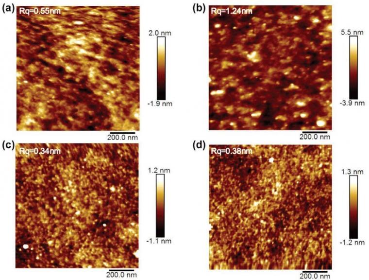
The a-Ga2O3 and Al2O3 surface morphologies, after being etched, is revealed by AFM (Figure 1). The root-mean-square (RMS) surface roughness of the as-deposited a-Ga2O3 (Figure 1a) film is 0.55 nm, which is slightly smaller than the 1.24 nm after etching (Figure 1b). In Figure 1c,d, the RMS values are 0.34 nm and 0.38 nm for unetched and etched Al2O3 films, respectively, indicating that the Al2O3 surface is uniformly etched by TMAH solution under this condition.
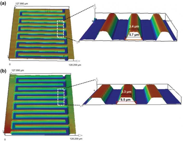
To further corroborate the effect of TMAH solution on the a-Ga2O3 patterns, 400 nm thick Ga2O3 films were patterned and etched into interdigitated features by etching with TMAH and H3PO4 solutions. Figure 2a,b shows the corresponding 3D laser scanning confocal microscope images collected in reflection mode, where well-defined patterns can be clearly seen in both cases. The cross-sectional views show the same trapezoidal structure, which is favorable for metal deposition. The ratios of the top to the bottom edges of the trapezoids are similar, demonstrating that the etching effect of TMAH is comparable with H3PO4. Thus, considering that TMAH barely etches metal or Al2O3, it is more preferred than H3PO4 for the fabrication of multi-component devices.
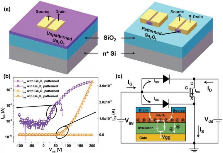
Based on the above-mentioned wet chemical etching technique using TMAH solutions, common bottom-gate TFTs with patterned and unpatterned a-Ga2O3 channels were fabricated on commercial SiO2/Si substrates (Figure 3a). The electrical characteristics are measured at a source-drain voltage (VDS) of 10 V with the source–gate voltage (VGS) from -100 V – 200 V (Figure 3b). The TFT with patterned a-Ga2O3 channel exhibits a typical n-type transfer curve. [17,18] The gate current (IGS), generally defined as leakage current, is very low, about 10-10 A for the entire VGS range. Conversely, the TFT with unpatterned a-Ga2O3 channel shows an abrupt drop of the drain current (IDS) in the transfer curve at a specific VGS, where the IGS begins to increase dramatically, indicating that the channel electrons start to transport vertically through SiO2 layer and reach the gate electrode at a positive VGS. The abnormal curves imply that it is beneficial to use a patterned a-Ga2O3 channel layer.
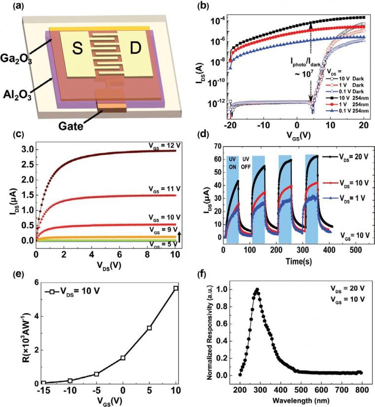
Next, an Al2O3 dielectric layer was used to fabricate a-Ga2O3 TFT with a bottom-gate staggered structure on quartz substrates. The interdigitated configuration is used to separate photogenerated carriers effectively.[1,19] A winding gate electrode was designed with a 1.5 μm overlap at the edge of the S/D electrodes (Figure 4a). Figure 4b shows the IDS–VGS transfer curves at different VDS in the dark and under 254 nm light illumination. The on-state IDS increases as VDS increases from 0.1 V to 10 V, and the off-state IDS remains low. The device exhibits decent electrical performance, such as a high on/off ratio of about 107, a low subthreshold swing of 0.65 mV dec-1 and a moderate positive threshold voltage (Vth) of 5 V. Under 254 nm light, the IDS increases in the depletion region compared with the in the dark. The on-state photocurrent also increases as VDS increases from 0.1 V to 10 V. At VDS = 10 V and VGS = 4 V, a high photocurrent of about 10-4 A is obtained, leading to a large light-to-dark current ratio of 5 × 10⁷.
The ultrahigh rejection ratio is reasonable because the depletion “off” state in the dark is reversed into an “on” state due to the presence of numerous photogenerated electrons.[20] Figure 4c demonstrates the output curves of the same device with an excellent linear and saturation performance, indicating a good ohmic contact between the Ga2O3 and Ti/Au. Time-dependent photoresponse behavior was evaluated with VGS = 10 V (Figure 4d). The IDS increases as VDS varies from 1 V – 20 V. Furthermore, the device demonstrates a relatively slow response to the periodic UV illumination. Figure 4e shows the responsivity (R) as a function of VGS at VDS = 10 V. R is calculated according to the following equation:

where Iphoto is the photocurrent, Idark is the dark current, P is the light intensity, and S is the illumination area. As VGS increases from −15 V– 10 V, R increases to 5.67 × 10³ A W-1. Based on this responsivity value, the detectivity (D*) expressed as:

is calculated to be 1.87 × 10¹⁵ Jones. A normalized photoresponse spectrum has been measured at VDS = 20 V and VGS = 10 V and shows a peak at 285 nm and a long tail until 360 nm. (Figure 4f)
Next, the suppression of PPC with the pulse gate voltage was investigated. A strong PPC remains for dozens or even hundreds of seconds in the a-Ga2O3 phototransistor working in a quasi-two-terminal configuration with VGS = 0 V, (Figure 5a), which severely hinders its practical applications. To diminish the PPC, a positive 20 V gate bias with a pulse width of 850 ms is applied. The IDS curve shows an instantaneous sharp peak and then immediately recovers to about 10−10 A once the gate voltage is reset to 0 V, suggesting that the PPC phenomenon is suppressed (Figure 5a,b). The decay time td, defined as the time during which the current decays from 90% to 10%, was 5 ms.
In this work, a highly selective etching solution was developed for the preparation of patterned a-Ga2O3 films using TMAH. A distinct influence of the chemical etching on device performance is investigated by comparison of two common bottom-gate TFTs with patterned and unpatterned a-Ga2O3. Furthermore, a bottom-gate a-Ga2O3 TFT was fabricated, with interdigitated S/D electrodes. The TFT shows typical n-type oxide semiconductor TFT transfer curves with a high on/off ratio of approximately 107, and excellent output characteristics. The device demonstrates a good response to UV 254 nm light, such as a high light-todark ratio of 5 × 10⁷ and responsivity of 5.67 × 10³ A W-1. Also, the PPC in a-Ga O-based phototransistors is effectively suppressed by applying a positive gate pulse with a decay time as low as 5 ms. These results suggest that the chemically etched a-Ga2O3 phototransistor is promising for high-performance UV photodetection and imaging applications.
References
This text is a digest version of:
Han, Z. Y., Liang, H. L., Huo, W. X., Zhu, X. S., Du, X. L., Mei, Z. X., Boosted UV Photodetection Performance in Chemically Etched Amorphous Ga2O3 Thin‐Film Transistors. Adv. Optical Mater. 2020, 8, 1901833. https://doi.org/10.1002/adom.201901833
[1] S. Cui, Z. Mei, Y. Zhang, H. Liang, X. Du, Adv. Opt. Mater. 2017, 5, 1700454.
[2] S.-J. Cui, Z.-X. Mei, Y.-N. Hou, Q.-S. Chen, H.-L. Liang, Y.-H. Zhang, W.-X. Huo, X.-L. Du, Chin. Phys. B 2018, 27, 067301.
[3] S. Cui, Z. Mei, Y. Hou, M. Sun, Q. Chen, H. Liang, Y. Zhang, X. Bai, X. Du, Sci. China: Phys., Mech. Astron. 2018, 61, 107021.
[4] N. Kumar, K. Arora, M. Kumar, J. Phys. D: Appl. Phys. 2019, 52, 335103.
[5] S. Jeon, S.-E. Ahn, I. Song, C. J. Kim, U.-I. Chung, E. Lee, I. Yoo, A. Nathan, S. Lee, K. Ghaffarzadeh,
J. Robertson, K. Kim, Nat. Mater. 2012, 11, 301.
[6] H. X. Jiang, J. Y. Lin, Phys. Rev. Lett. 1990, 64, 2547.
[7] D. Ye, Z. Mei, H. Liang, L. liu, Y. Zhang, J. Li, Y. Liu, C. Gu, X. Du, Sci. Rep. 2016, 6, 26169.
[8] H. Liang, S. Cui, R. Su, P. Guan, Y. He, L. Yang, L. Chen, Y. Zhang, Z. Mei, X. Du, ACS Photonics 2019, 6, 351.
[9] A. Jacnotti, C. G. Van de Walle, Phys. Rev. B 2007, 76, 165202.
[10] Y. Qin, H. Dong, S. Long, Q. He, G. Jian, Y. Zhang, X. Zhou, Y. Yu, X. Hou, P. Tan, Z. Zhang, Q. Liu, H. Lv, M. Liu, IEEE Electron Device Lett. 2019, 40, 742.
[11] Y. Qin, S. Long, Q. He, H. Dong, G. Jian, Y. Zhang, X. Hou, P. Tan, Z. Zhang, Y. Lu, C. Shan, J. Wang, . Hu, H. Lv, Q. Liu, M. Liu, Adv. Electron. Mater. 2019, 5, 1900389.
[12] W. Kim, K. S. Chu, Phys. Status Solidi A 2009, 206, 179.
[13] J. Lee, K.-H. Lim, Y. S. Kim, Sci. Rep. 2018, 8, 13905.
[14] K. Seong, K. Kim, S. Y. Park, Y. S. Kim, Chem. Commun. 2013, 49, 2783.
[15] S. Ohira, N. Arai, Phys. Status Solidi C 2008, 5, 3116.
[16] T. Oshima, T. Okuno, N. Arai, Y. Kobayashi, S. Fujita, Jpn. J. Appl. Phys. 2009, 48, 040208.
[17] T. Kamiya, K. Nomura, H. Hosono, Sci. Technol. Adv. Mater. 2010, 11, 044305.
[18] R. A. Street, Adv. Mater. 2009, 21, 2007.
[19] L.-X. Qian, Z.-H. Wu, Y.-Y. Zhang, P. T. Lai, X.-Z. Liu, Y.-R. Li, ACS Photonics 2017, 4, 2203.
[20] H. S. Bae, M. H. Yoon, J. H. Kim, S. Im, Appl. Phys. Lett. 2003, 83, 5313.
Copyright
Z. Han, H. Liang, W. Huo; Advanced Optical Materials; DOI: 10.1002/adom.201901833;
© 2020 WILEY-VCH Verlag GmbH & Co. KGaA, Weinheim
Source: Preview Image: Matej Moderc/Getty Images