Native Oxide Barrier Layer for Selective Electroplated Metallization of Silicon Heterojunction Solar Cells
Introduction
Electroplated copper contacts are particularly attractive for crystalline silicon heterojunction (SHJ) solar cells, which require a low-temperature metallization. Current trends in the silicon photovoltaic field point toward passivated contact architectures for high-efficiency solar cells.[1, 2]
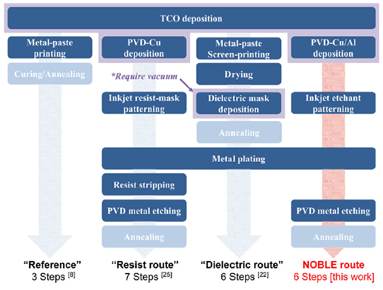
The symmetrical SHJ solar cell architecture is created by first depositing a thin intrinsic amorphous hydrogenated silicon layer – i.e., a-Si:H(i) onto the cleaned and textured c-Si wafer, followed by the doped a-Si:H (n or p), which act as carrier-selective junction. Both ultra-thin a-Si layers are quite sensitive to process temperatures above 200 °C (392 °F).[3] Typically, a transparent conductive oxide (TCO) is sputtered onto the a-Si:H layers to contact the silicon, promote the lateral conductivity in the solar cell, and to serve as an antireflective coating. The cell architectures then need to be contacted by metallization approaches, where metal paste printing is the most common [PG1] and metal plating offers promising alternatives. Figure 1 presents an overview of the low-temperature routes to metallize SHJ solar cells covered by TCO.
Our work demonstrates an alternative plating approach containing one step less than the “Resist Masking route” and uses very low amount of silver (Ag). Our novel native oxide barrier layer for selective electroplating (“NOBLE route”) aims at improving the process flow with fewer steps and by avoiding the use of any costly organic masks. In this concept, the native oxide of a thin aluminum (Al) layer enables performing selective copper (Cu) plating onto a patterned metal seed. An etchant is inkjet-printed to structure the contact positions in the Al layer. This grid-patterning method is even cheaper than the deposition of a reactive silver ink onto the aluminum.[4, 5]
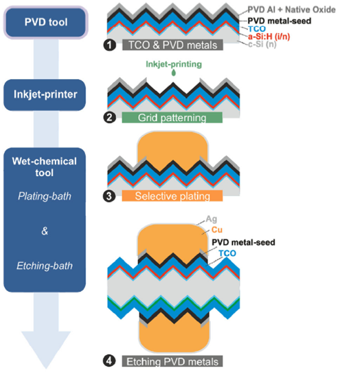
The NOBLE metallization route depicted in Figure 2 allows fast and homogeneous electrodeposition of copper onto a multifunctional patterned metal layer.
After vacuum deposition of the PVD layer stack (Figure 2(1)), the grid patterning is achieved by printing a low concentrated alkaline ink or paste to etch the aluminum-aluminium oxide (Al-Al2O3) selectively (Figure 2(2)). In the present work, inkjet printing was employed. This selective etching removes the Al layer only in grid positions and does not impact the underlying metal-seed (on top of the TCO). This patterning step allows plating Cu selectively onto the metal seed (Figure 2(3)). At this state, the less noble metal Al and the Al2O3 are acting as barrier to inhibit Cu plating in the non-grid positions as described by Hatt et al.[5] A thin silver capping (≈200 nm) follows to protect the Cu-contacts against oxidation. The remaining PVD layers (Al and metal seed) in non-grid positions are then etched-back by chemical processing without damaging the underlying TCO (Figure 2(4)). On the contact flank, only a few nanometers of Cu are not protected by Ag in comparison to the “Resist route,” which leaves several micrometers un-capped.
Methods
Investigations on metal etching were realized on planar glass (soda-lime glass) with different sputtered metals (Al, Cu, Ag, NiV (93:7), and Ti) Electron-gun evaporation was also used to deposit Al onto glass to observe the impact of the PVD technique on the etching rate for this metal. The metal thicknesses were measured before and after etching using an Olympus LEXT OLS4000 confocal microscope, a profilometer (Dektak - Stylus Profiler), or an X-ray fluorescence tool.
After sputtering the metallic layers onto the SHJ solar cells, a PIXDRO LP50 printer from Meyer Burger Technology AG was used to print the grid positions with NaOHaq, thus completely etching the Al. A complete description of the cell fabrication process can be found in the original work. The contact metallization was characterized by the Olympus LEXT OLS4000 confocal microscope after each processing step.
Results and Discussion
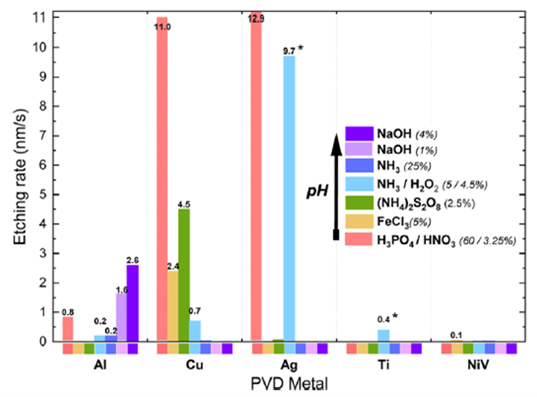
The etching selectivity of different metals was studied to enable the selective etching steps mentioned above. There are many solutions that may etch metals deposited by PVD. The investigation was focused on PVD Al, Ti, NiV, Cu, and Ag, which are promising for either low-contact resistance or plating selectivity. The etch rates in nm s-1 are presented in Figure 3 for metals sputtered on planar glass. Although etching rates might be different on different surfaces, general trends were confirmed to be similar on TCOs and on the textured surface of the SHJ solar cells.
In summary, it was observed that Al can be selectively removed versus Cu or Ag with dilute alkaline solutions and at high etching rates. On the other hand, Cu can be etched with FeCl3 or (NH4)2S2O8, while Ag and Al will remain unaffected.
For the NOBLE processing, both sides of the textured SHJ precursor with ITO are entirely covered by thin layer stacks of either PVD-Cu/Al (50/100 nm) or Ag/Al (20/100 nm). The selective etching of Al against the metals below (Cu or Ag) enables easy patterning of the grid positions. In the present work, inkjet-printing of NaOHaq was employed to structure lines in the Al-Al2O3 layer. Narrow lines in the PVD Al of around 25 μm wide without spreading or interruption were created. The underlying PVD Cu-seed can be observed in line positions as demonstrated in Figure 4a.
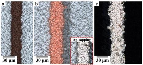
The selective Cu electrodeposition is then performed onto the Cu-seed as observed in Figure 4b. The native oxide, covering the Al surface, acts as inhibitor for Cu deposition outside of the designated contact area. The Cu grows isotropically onto the metal seed, which widens the contact a bit. The Cu deposition is fine-granular, which gives high contact conductivity near the value of the Cu-bulk. A thin silver capping is also deposited to prevent Cu from any oxidation, as seen on the inset.
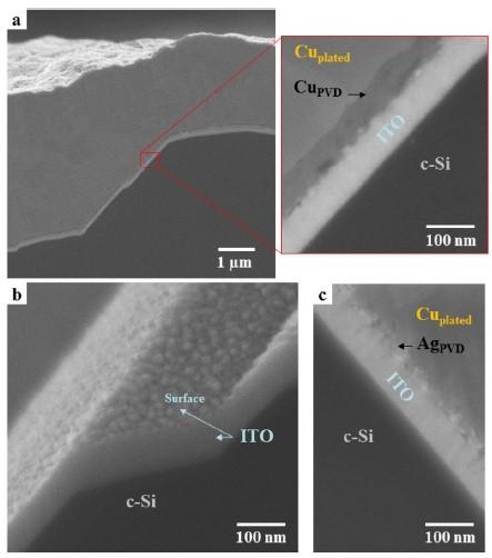
After plating, the PVD layers are selectively etched back (Figure 4c) in non-grid positions with a solution of H3PO4/HNO3. SEM images of the fingers’ cross-sections (Figure 5) confirms that ITO was not significantly damaged through the etch-back step, and the layers presented good adhesion even with non-optimized conditions. No voids or uncontacted area could be detected, which would increase the resistivity at the interface. Good adhesion was also confirmed by tape testing.
Sheet resistances (Rsh) of ITO and contact resistivities (ρc) measured on both sides of different stacks after NOBLE metallization are summarized in Table 1. The measured ρc shows little difference between PVD metal seed composed by Cu or Ag, which means the use of Cu-seeds can be an efficient way of cost reduction, getting closer to Ag-free metallization. Moreover, our contact stack after NOBLE metallization present similar results to the one used by CSEM to reach a very high efficiency up to 24.1% on a bifacial plated SHJ solar cell.[6]
Table 1. Sheet resistances (Rsh) of ITO and contact resistivities (ρc) of different stacks measured by TLM after NOBLE metallization on commercial SHJ solar cells.
Metal stack | Rsh [Ω sq-1] | ρcontact [mΩ cm2] | |
c-Si (n)/a-Si:H(i/n)/ITO/CuPVD/Cu-Agplated | 82.7 ± 0.2 | 4.0 ± 0.4 |
|
c-Si (n)/a-Si:H(i/n)/ITO/AgPVD/Cu-Agplated | 80.6 ± 0.2 | 3.5 ± 0.8 |
|
c-Si (n)/a-Si:H(i/p)/ITO/CuPVD/Cu-Agplated | 169.7 ± 0.5 | 2.8 ± 0.5 | Not influenced by the bulk |
c-Si (n)/a-Si:H(i/p)/ITO/AgPVD/Cu-Agplated | 120.3 ± 0.4 | 1.8 ± 0.3 | |
SHJ solar cell made with NOBLE metallization presented efficiency (η) of 20.2% and an encouraging fill-factor (FF) of 78.0% was obtained. This is despite the fact that the pseudo fill factor (pFF) of this cell is already limited to only 80.5%, due to the small cell size. Table 2 presents the SHJ solar cell properties under 1-sun illumination.
Table 2. SHJ solar cell properties after NOBLE metallization.
Area [cm2] | Voc [mV] | pFF [%] | FF [%] | Jsc [mA cm-2] | η [%] |
6.25 | 718 | 80.5 | 78.0 | 36.1 | 20.2 |
The open-circuit voltage Voc and pseudo fill-factor pFF limitations result from the non-optimized metal sputtering process on ITO and from the small cell size. The fill factor is impacted by the non-optimal grid design. The short-circuit current Jsc might be reduced by the lab-scale etch-back procedure of the PVD layers. Optimizations of the process might exploit further the full potential of the solar cell in combination with the apparently well performing metallization.
Conclusion
An alternative approach for low-temperature metallization of solar cells with TCO layer (e.g., SHJ solar cells), which is currently in the early development stage, was demonstrated. It takes advantage of the selectivity of etchants and plating processes toward different metals.
A thin stack of two PVD metal layers were sputtered onto the cell right after the TCO in the same tool without breaking the vacuum. Thus, sputtering costs are kept low, especially for these thin layers and materials such as Al and Cu. These metal layers allow plating the patterned contacts on both sides of the cell at the same time quickly and homogeneously. The selective etching of metals was investigated in a study of etching rates for Al, Cu, Ag, Ti, and Ni in different acidic and alkaline solutions. This selectivity enabled grid patterning of a thin PVD-Al layer by inkjet printing of an alkaline solution. Copper could then be plated in the printed areas, without parasitic deposition, onto the underlying PVD metal-seed due to the presence of native oxide on the Al surface. After electroplating, the thin PVD layers were removed by etching in non-grid positions selectively. Contact resistivity below 3 mΩcm2 were achieved on stack systems of ITO-CuPVD-Cuplated-Agplated, and the improvement of the sputtering might allow reaching 0.4 mΩcm2, as reported in the literature. A promising efficiency of 20.2% with a FF of 78.0% was presented on a commercial SHJ solar cell precursor. This approach saves processing steps and consumables as compared to the electroplating into openings in an organic mask.
Literature
[1] M. A. Green, Y. Hishikawa, E. D. Dunlop, D. H. Levi, J. Hohl-Ebinger, A. W. Y. Ho-Baillie, Prog Photovolt. Res. Appl. 2018, 26, 427.
[2] K. Yoshikawa, H. Kawasaki, W. Yoshida, T. Irie, K. Konishi, K. Nakano, T. Uto, D. Adachi, M. Kanematsu, H. Uzu, K. Yamamoto, Nat. Energy 2017, 2, 17032.
[3] B. Demaurex, S. de Wolf, A. Descoeudres, Z. Charles Holman, C. Ballif, Appl. Phys. Lett 2012, 101, 171604.
[4] M. Glatthaar, R. Rohit, A. Rodofili, Y. J. Snow, J. Nekarda, J. Bartsch, IEEE J. Photovoltaics 2017, 7, 1569.
[5] T. Hatt, V. P. Mehta, J. Bartsch, S. Kluska, M. Jahn, D. Borchert, M. Glatthaar, AIP Conf. Proc. 2018, 1999, 40009.
[6] A. Lachowicz, J. Geissbühler, A. Faes, J. Champliaud, F. Debrot, E. Kobayashi, J. Horzel, C. Ballif, M. Despeisse (Eds.), Copper Plating Process for Bifacial Heterojunction Solar Cells: 33rd European Photovoltaic Solar Energy Conf. Exhibition; 2017, 753–756.
Original Publication:
T. Hatt, S. Kluska, M. Yamin, J. Bartsch, M. Glatthaar, Sol. RRL. 2019, 3, 1900006. DOI: 10.1002/solr.201900006
Source: Preview Image: MACIEJ NOSKOWSKI/iStockphoto