Spray-Coated Polymer Solar Cells Based on Low-Band-Gap Donors Processed with ortho-Xylene
Introduction
Polymer solar cells (PSCs) have attracted the attention of the scientific community because they offer the possibility to fabricate photovoltaic devices by solution processing, enabling a reduction in cost and increase in their potential for application in fields such as consumer electronics and building-integrated photovoltaics (BIPVs).[1, 2] In recent years, marked improvement was made possible by the use of photoactive layers based on low-band-gap polymers, which allow better harvesting of solar energy compared to the conventionally used material poly(3-hexyl-thiophene) (P3HT). In particular, poly{[4,8-bis-(2-ethyl-hexyl-thiophene-5-yl)-benzo[1,2-b:4,5-b’]dithiophene-2,6-diyl]-alt-[2-(20-ethyl-hexanoyl)-thieno[3,4-b]thiophen-4,6-diyl]} (PBDTTT-C-T) in combination with PC70BM is an effective blend system that reaches high efficiency.[3–5]
In spite of this remarkable progress, a strong limitation that hinders the scaling-up of PSC fabrication is the use of chlorinated solvents (toxic toward human health and the environment), which serve to effectively dissolve the polymer/fullerene blend to obtain a suitable morphology. Hence, blends dissolved in more eco-friendly solvents have attracted significant interest.
We report on the use of a PBDTTT-C-T:PC70BM composite dissolved in ortho-xylene, and deposited both via spin-coating and spray deposition, in direct PSCs. A record conversion efficiency of 8% is achieved by devices with the spin-coated blend, whereas the devices with the spray-coated blend reach an efficiency of 4.4% after proper optimization of the spray parameters.
Methods
The photovoltaic devices were fabricated on ITO-coated glass substrates. The electron transport layer was PEDOT:PSS VPAI 4083. The PBDTTT-C-T and PC70BM blend (1:1.5) were dissolved in ortho-xylene. Undiluted and diluted blends with and without di-iodooctane (DIO) were prepared before deposition.
Glass/ITO substrates were patterned by wet etching. PEDOT:PSS was spin-coated in a glove box and then dried by thermal annealing at 150 °C (302 °F) for 10 minutes in a nitrogen atmosphere. PBDTTT-CT:PC70BM was either spin-coated or sprayed by using a dual-action commercial airbrush supplied by compressed air. After drying, the samples were completed by thermal evaporation of 10 nm of calcium and 100 nm of aluminum in high vacuum.
Optical images of the deposited photoactive layers were acquired by using an Olympus® LEXT™ OLS4000 microscope. The thicknesses of the as-deposited films were measured with a profilometer (Dektak 150). The surface topography was monitored using an A.P.E. Research AFM. Absorption curves were obtained by a UV-VIS-NIR spectrophotometer (Shimadzu UV2550). A custom-made tool comprising a sourcemeter (Keithley, mod.2612) and a monochromator (Newport, Mod.74000) was used to measure the external quantum efficiency (EQE) values of the photovoltaic cells. J–V curves of the devices were evaluated by using a class A solar simulator (ABET Technologies, Sun2000). Before each measurement, the irradiation level at the height and position of the solar cell was verified by a means of a calibrated pyranometer (SkyeSKS1110).
Results and Discussion
A preliminary investigation was carried out to choose the different solution formulations for spin and spray deposition in order to obtain suitable layers of the PBDTTT-C-T:PC70BM blend dissolved in ortho-xylene. We found that the solution used for spin-coating was also applicable for the spray technique; in fact, the pure solution was not viscous and easy to spray. However, we also investigated a diluted solution (1:4) to determine the effect of dilution on film-forming properties of the spray-coated samples. Blend deposition was performed by using blends both with and without di-iodooctane (DIO) in order to understand the influence of the additive on the morphology of PBDTTT-CT:PC70BM dissolved in ortho-xylene.
Figure 1 shows an optical analysis of the active layers. The DIO additive evidently enhances the surface morphology of the photoactive layer, which should result in a better performance compared to the cases without DIO. In fact, when DIO is not added, large agglomerates of non-dissolved fullerene are visible in the spin-coated films, whereas in the spray-coated ones, there is no coalescence among the droplets, with most of them surrounded by coffee rings. Focusing on the diluted blend, DIO improves the appearance of the surface morphology of the film but coalescence is not at an advanced stage, leading to the deposition of visible droplets that are homogenous in composition but still different in size. Some uncovered areas are noticeable in the layer obtained using the undiluted blend with DIO, suggesting that it is difficult to obtain perfectly uniform coverage by spraying the blend for a few seconds.
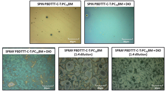
A deeper investigation of the surface topography was performed by atomic force microscopy (AFM). The corresponding root-mean-square (RMS) roughness values and layer thicknesses were measured by profilometry and are reported in Table 1. Topographies of spin- and spray-coated active layers without DIO are similar and present low roughness. The addition of DIO increases the RMS roughness of both spin and spray-coated films; in particular, for sprayed layers, the diluted blend with DIO exhibits larger, differently sized domains, showing higher roughness than the diluted blend without DIO. Notably, the RMS roughness is very low in spray-coated PBDTTT-C-T:PC70BM (1:4 dilutions) because the AFM measurement covers only a small area within the large (tens of micrometers) droplets shown in Figure 1 and does not consider the overall topography, which includes the solid content of droplet boundaries, and thereby underestimates the measurement. Regarding thickness, spin-coated active thickness increased with addition of DIO, which can be attributed to the higher viscosity of the modified solution.[6] Meanwhile, the spray-coated blends with and without DIO have similar thicknesses.
Table 1: Thickness and root-mean-square (RMS) roughness of the active layers with various blend formulations and deposition techniques.
Active Layer | Deposition | Thickness | RMS |
PBDTTT-C-T:PC70BM | spin | 100 | 1.52 |
PBDTTT-C-T:PC70BM + DIO | spin | 130 | 3.85 |
PBDTTT-C-T:PC70BM + DIO | spray | 122 | 2.90 |
PBDTTT-C-T:PC70BM (1:4 dilution) | spray | 126 | 1.76 |
PBDTTT-C-T:PC70BM + DIO (1:4 dilution) | spray | 120 | 18.8 |
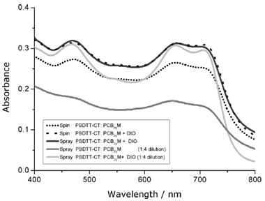
Absorbance spectra (Figure 2) show a greater absorption when DIO is added to the solutions; also, the spectra for the undiluted solutions with DIO used both for spin- and spray-coating match very closely. Regions of lower absorption are apparent in the 1:4 diluted solution with DIO. Because the thicknesses are approximately the same as in the undiluted spray-coated layer, this decrease may be due to the use of a non-optimized DIO concentration. The lower intensities of the sprayed diluted active layer without DIO suggest a poor morphology of the phase-separated bulk heterojunction (BHJ) materials.
In Table 2 we summarize the photovoltaic performance of the described blend formulations and deposition techniques in terms of short-circuit current density (JSC), open-circuit voltage (VOC), fill factor (FF), and power conversion efficiency (PCE). The film-forming properties of the various solutions deposited by spin and spray-coating, with and without DIO, are clearly correlated to the observed photovoltage in the finished cells. VOC is high only in the presence of DIO, revealing that such an additive is essential in achieving a favorable morphology and proper coverage of the surface, in agreement with the optical analysis in Figure 1. An abrupt decrease of fill factor occurred in the case of spin and spray-coated active layers without DIO, and this may be caused by the poor bulk nanometer-scale morphology. In addition, in the spray-coated layer the droplet boundaries (as evident in Figure 1) hinder charge transport, leading to a high series resistance that heavily affects the JSC and the FF values.
Table 2. Electrical performance of the best fabricated devices from various blend formulations and deposition techniques. Average values and standard deviations over eight devices are reported in parentheses.
Active Layer | Deposition | Voc [V] | Jsc [mA cm-2] | FF | PCE [%] |
PBDTTT-C-T:PC70BM | spin | 0.57 | 5.6 | 0.35 (0.33±0.02) | 1.1 (0.84±0.33) |
PBDTTT-C-T:PC70BM + DIO | spin | 0.78 | 16.2 | 0.65 (0.63±0.01) | 8.0 (7.39±0.34) |
PBDTTT-C-T:PC70BM + DIO | spray | 0.72 | 12.2 | 0.50 (0.48±0.01) | 4.4 (3.8±0.55) |
PBDTTT-C-T:PC70BM (1:4 dilution) | spray | 0.39 | 4.8 | 0.32 (0.31±0.005) | 0.5 (0.48±0.04) |
PBDTTT-C-T:PC70BM + DIO (1:4 dilution) | spray | 0.7 | 9.6 | 0.44 (0.38±0.03) | 2.7 (2.03±0.47) |
Comparing the performance obtained using the additive in PBDTTT-C-T:PC70BM both for spin and spray-coating, an enhancement of the photo-generated current is observed. This enhancement can be ascribed to improved charge transport at the interface, corresponding to a larger surface roughness (as shown by the RMS values in Table 1) that implies a more uniform distribution of the domains on the active layer’s surface.[6] The different values of JSC observed in the diluted and undiluted cases suggest that the dilution does not achieve the same uniformity in the thickness of the active film, as confirmed by the very large value of roughness in the diluted film. Moreover, the photocurrent is affected by resistive losses (high series resistance).
Remarkable electrical performance is obtained from the device based on the undiluted blend deposited by spray-coating, but it is lower than those from a device using the same blend applied by spin-coating. We ascribe this difference to the spray environment (air) and to non-optimal coverage due to short spraying time. Focusing on the data in the Table 2, a satisfactory reproducibility is observed both for spin- and spray-coating in the case of the undiluted blend, and for spray-coating in the case of the diluted blend. This demonstrates the good control over the process and the ability to generate good coverage by using solutions with different formulations in two different techniques (see Figure 1), providing reliable electrical results.
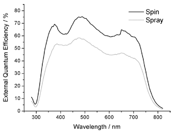
Figure 3 shows the external quantum efficiency (EQE) spectra of the best-performing devices fabricated with the spin- and spray-coated active layers. Although the solution used to deposited both the layers is the same (PBDTTT-C-T:PC70BM + DIO), the EQE for the spray-coated layer is lower than that of the spin-coated layer, explaining the lower JSC values; moreover, at short wavelengths the peak associated to PC70BM absorption is not so distinct and at longer wavelengths the profile is decreased, probably due to the lack of a uniform coverage which influences the blend/evaporated contact interface.
The difference between the devices with spin-coated and spray-coated layers is still large, but this work opens the way to the use of low-band-gap materials in spray-coating, a non-wasteful technique that is compatible with large areas and potentially effective for the fabrication of organic photovoltaic devices.
Conclusion
We report the results of a study on the behavior of spin- and spray-coated PBCDTTT-C-T:PC70BM active layers, both pristine and with an amount of additive (DIO), to fabricate bulk heterojunction polymer solar cells. This work highlights the critical issues of the spray-coating technique in relation to the use of a low-band-gap polymer. However, we achieve promisingly high efficiencies of 8% for a spin-coated PBCDTTT-C-T:PC70BM layer and 4.4% for a spray deposited layer, both processed in a non-chlorinated solvent in ambient atmosphere. We also demonstrate the importance of the solution used in the improvement of the film quality and the compatibility with large-area processes. Those results are promising to produce organic solar cells with non-chlorinated solvents at low temperatures and low costs.
Literature
[1] N. Espinosa, M. Hosel, D. Angmo, F. C. Krebs, Energy Environ. Sci. 2012, 5, 5117.
[2] T. D. Nielsen, C. Cruickshank, S. Foged, J. Thorsen, F. C. Krebs, Solar Energy Mater. Solar Cells 2010, 94, 1553–1571.
[3] X. Guo, M. Zhang, W. Ma, L. Ye, S. Zhang, S. Liu, H. Ade, F. Huang, J. Hou, Adv. Mater. 2014, 26, 4043–4049.
[4] X. Fan, G. Fang, F. Cheng, P. Qin, H. Huang, Y. Li, J. Phys. D 2013, 46, 305106.
[5] P. Adhikary, S. Venkatesan, N. Adhikari, P. P. Maharjan, O. Adebanjo, J. Chenb, Q. Qiao, Nanoscale 2013, 5, 10007–10013.
[6] H.-Y. Chen, S.-H. Lin, J.-Y. Sun, C.-H. Hsu, S. Lan, C.-F. Lin, Nanotechnology 2013, 24, 484009.
Original Publication:
L. La Notte, G. Polino, C. Ciceroni, F. Brunetti, T. M. Brown, A. Di Carlo, A. Reale, Energy Technol. 2014, 2, 786-791. DOI: 10.1002/ente.201402059
Source: Preview Image: Petmal/Getty Images