Atomic Force Microscopy Analysis of Aluminum Layer Properties and Correlation to Masking Functionality in Copper Plating Metallization for Solar Cells
Abstract
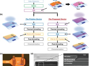
The native AlOx grown on a thin sputtered aluminum layer can be used as mask for electroplating copper, e.g., for metallizing silicon heterojunction (SHJ) solar cells. Effects that influence the masking quality for selective electroplating are studied herein. Atomic force microscopy characterization in PeakForce mode highlights the presence of some insulation defects in the native AlOx due to local contamination, pinholes, or tunneling currents. A focused ion beam/scanning electron microscopy analysis is further conducted to understand some defects in detail. The AlOx insulation can be improved by adsorbing a self-assembled monolayer, which is mainly required along the process sequence to adjust the surface wetting of the Al for optimal NaOHAq printing. The mask quality and complete metallization sequence for solar cells are demonstrated on industrial SHJ precursors. Inkjet- and FlexTrail-printing of NaOHAq are shown to be suitable to pattern the Al layer. Promising conversion efficiency comparable to screen-printing reference is reached on large area.


