Surface-Dependent Properties and Tunable Photodetection of CsPbBr3 Microcrystals Grown on Functional Substrates
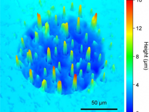
All-inorganic metal halide perovskites are highly attractive materials for optoelectronics and are typically implemented as thin films, nanocrystals, and single crystals with macroscopic and millimeter-size dimensions. Single crystals with regular shapes in the micrometer range are less explored and present an interesting alternative when a well-defined and spatially localized response is desired. Here, CsPbBr3 microcrystals are fabricated by simple and fast drop-casting of a precursor solution on several substrates that for the growth process are heated to temperatures in the range from 80 to 150 °C. The microcrystals have a cubic shape and feature a pyramidal cavity on their top surface that forms due to faster growth at the edges once the growing crystal is attached to the substrate. Distinct heterogeneity in the photoluminescence (PL) and conductivity of the different facets are measured by µ-PL and conductive atomic force microscopy experiments. Toward device applications, the authors contact single microcrystals on conductive substrates mechanically with a micromanipulator tip. They observe diode-like current–voltage curves and good photodetector functionality, obtaining a high responsivity of 150–300 A W−1 in the blue–green spectral region under forward bias, and a sharp detection band centered around 540 nm with peak responsivity close to 0.7 A W−1 under reverse bias.


