State of the Art Methods and Applications of 3D Roughness and Dimensional Measurements
November 25, 2020 | 2-3 pm CET | 8-9 am EST
Part I: State of the art in traceable industrial 3D roughness and dimensional measurement using optical 3D microscopy and optical distance sensors
Dr. Uwe Brand
Head of the section Surface Metrology, German National Institute of Metrology, Braunschweig, Germany
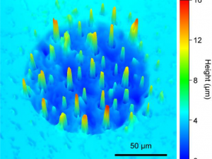
Optical measuring systems are widespread in surface and coordinate metrology. They are fast with high resolution, contactless and therefore non-destructive. These aspects are essential for the factory of the future. Unfortunately, optical measurements are often not traceable to the Si units due to the complexity of the interaction between measurand and measuring system. A recent European comparison measurement on areal roughness standards reveals strong differences in measured roughness parameters, which are much larger than the stated measurement uncertainties. Likewise, optical diameter measurements at 200 µm Rockwell indenters with confocal microscopes showed deviations up to 3 µm compared to reference instruments. This contribution will present the state of the art for four different types of instruments: confocal microscopes, coherence scanning interferometry instruments, focus variation microscopes and optical distance sensors on coordinate measuring machines. Routes to support industry in traceable roughness and dimensional metrology will be highlighted together with ideas on how to characterize optical instruments and to investigate the influencing factors arising from the different optical working principles, optical instrumentation setup and feature properties.
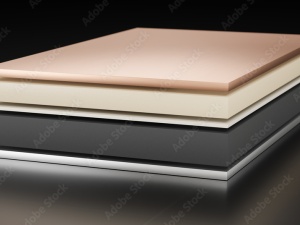
Part II: A smooth transition to 5G: Why geometry and roughness testing is critical in 5G PCB manufacturing
Markus Fabich
Strategic Marketing Manager,Olympus, Hamburg, Germany
On the journey towards industry 4.0, autonomous driving and the internet of things, rollout of 5G technology is one of the key milestones. With the implementation of 5G, requirements for PCB manufacturing change considerably due to the higher signal frequencies. This has implications for the IQ/OQ/PQ journey.
In this webinar, you will get an insight into the rationale of 5G PCB manufacturing and why this has an impact on the whole business infrastructure. We will discuss the emerging importance of roughness testing of conductor tracks, as well as state-of-the-art inspection workflows for precision roughness testing.
You can ask questions at any time during the webinar. Questions will be answered during the Q&A session.
Who should attend the Webinar?
This webinar is aimed at (among others) researchers, process owners and members of quality departments in the electronics sector.
Key Learning Objectives
- What is the skin effect?
- Why is it relevant for conductivity?
- What is important to consider in terms of process control?
- How to obtain the right control parameters with regard to roughness