In Situ Integration of SERS Sensors for On‐Chip Catalytic Reactions
The rapid progress of microfluidics has contributed to modern analytical methodology. However, in situ integration of chemical/biological sensors for on‐chip reaction monitoring remains a big challenge. Here, a graphene‐based catalytic chip with surface‐enhanced Raman scattering (SERS) sensors was fabricated by laser scribing of a graphene oxide (GO)–silver nanoparticle (AgNP) composite (AgNPs@GO). The surface plasmonic effect of AgNPs promoted the photoreduction of GO (RGO), inducing a highly porous nanostructure. By combining the AgNPs@RGO composite patterns with polydimethylsiloxane microfluidic channels, a bifunctional microfluidic chip was fabricated capable of on‐chip catalysis and SERS detection. As a proof‐of‐concept demonstration, on‐chip AgNP‐catalyzed 4‐nitrophenol reduction was performed while the reaction process was monitored by the in situ SERS sensor. The integration of SERS sensors with functional microfluidic devices holds great promise for developing advanced Lab‐on‐a‐Chip systems.
Introduction
Lab‐on‐a‐Chip (LoC) systems are highly integrated devices allowing multiple experimental procedures, including sample injection, reaction handling, product separation, and component analysis, on a single chip [1]. The ultra‐low consumption of fluids makes LoC favorable in medical diagnostics, environmental monitoring, and chemical analysis [2–4]. To further extend the functionalities of LoC devices, various functional components have been successfully integrated with microfluidic chips, which significantly facilitated automatic analysis [5]. Nevertheless, most of these proof‐of‐concept devices cannot be applied in real production as the fabrication of these multifunctional LoCs generally involves complex manufacturing procedures [6]. The channel networks need to be specially designed, and the on‐chip fabrication techniques are usually highly precise 3D nanotechnologies that are not yet fully developed for market‐oriented commercialization. Therefore, realizing multi‐functionalization on a single chip remains a big challenge.
Laser scribing technology that converts near‐infrared light (NIR, ≈780 nm) inside a digital versatile disc (DVD) drive into localized heat is a cost‐effective and simple tool for flexible patterning of graphene and many composite materials [7]. Laser‐scribed graphene oxide (GO) has been widely used to produce electronic devices because of its good mechanical properties, high electrical conductivity, and high surface area [8]. Thus, laser scribing of GO is promising for fabricating graphene‐based chemical sensors, actuators, and various electronics, which may contribute to the development of microfluidics. However, laser scribing of GO has not been fully applied to LoC functionalization.
In this study, a surface‐enhanced Raman scattering (SERS)‐active catalytic chip was fabricated by laser scribing of GO/silver nanoparticle composites (AgNPs@GO). The surface plasmonic effect of AgNPs promoted the photoreduction of GO, leading to a highly porous nanostructure. The well‐exfoliated graphene served as an excellent catalytic scaffold for AgNPs. The dense distribution of AgNPs on the laser‐scribed graphene led to a plasmonic structure, making the microfluidic chip SERS-active. Combining a catalyst bed with the SERS substrate enabled on‐chip catalysis and in situ SERS monitoring of 4-nitrophenol (4-NP) reduction. Thus, integrating SERS sensors with functional microfluidic devices holds great promise for developing advanced LoC systems in the future.
Methods
The composites AgNPs@GO‐1–3 were prepared by UV photoreduction. Briefly, GO (10 mL, 4 mg mL−1) was mixed with different amounts (5, 10, and 15 mL) of Ag(NH3)2OH, and the resulting solution was irradiated under UV‐light (500 W) for 10 min. The final composites were obtained after washing with deionized water.
Each AgNPs@GO composite (20 mL) was cast onto a LightScribe‐enabled disc to obtain a homogenous film. The disc was then inserted into a laser-scribe-enabled DVD drive equipped with an NIR laser (780 nm), and predesigned patterns of channel networks were directly "written" onto the composite film. Each AgNPs@GO composite was reduced to AgNPs@RGO (RGO, reduced GO) during laser scribing.
Laser‐scribed AgNPs@RGO was selectively transferred to a polydimethylsiloxane (PDMS) substrate by simple stamping. A PDMS microfluidic layer with conformal channel networks was then combined with the SERS‐active PDMS substrate, and the two PDMS layers were sealed together to create an SERS‐active catalytic chip.
For SERS detection, the laser power on the samples was adjusted to ≈30 µW, and the average spot size was 1 µm in diameter using a long‐working distance 50 × objective. SERS spectra were recorded on an instrument equipped with a liquid‐nitrogen‐cooled argon-ion laser at 532 nm using an exposure time of 5 s and three accumulations.
The composites were characterized by scanning electron microscopy (SEM), high-resolution transmission electron microscopy (HRTEM), and X-ray photoelectron spectroscopy (XPS). Confocal laser scanning microscopy (CLSM) images were obtained with an Olympus LEXT OLS4100 3D measuring laser microscope.
Results and Discussion
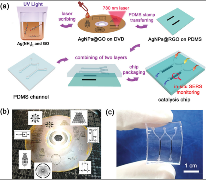
Figure 1a shows the fabrication procedure of the catalytic chip and in situ integration of the SERS sensors. Due to the photothermal effect of GO and the plasmonic effect of AgNPs, GO was effectively reduced (AgNPs@RGO) by laser irradiation. Various complex channels were patterned on the composite (Figure 1b). After laser irradiation, the compact AgNPs@GO film was exfoliated into a highly porous structure so that the resulting patterned AgNPs@RGO could be easily transferred onto a PDMS substrate by simple stamping. The PDMS substrate was then combined with another conformal channel layer, and a flexible catalytic chip with in situ SERS sensors was fabricated (Figure 1c). The chip was integrated with a catalyst bed capable of SERS monitoring.
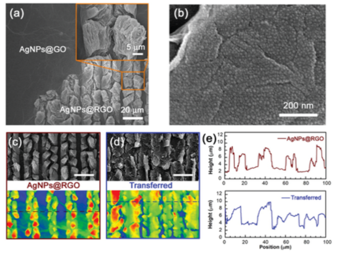
The morphology of the AgNPs@GO film was investigated before and after laser scribing (Figure 2a). The original AgNPs@GO film was compact and had a smooth surface, whereas laser‐scribed AgNPs@RGO was expanded and exfoliated, providing many active sites for the subsequent catalytic reaction and SERS detection. SEM of the AgNPs@RGO material indicated that AgNPs were uniformly distributed on the wrinkled RGO sheet (Figure 2b). The average size of AgNPs was ≈10 nm, and the gap between particles was ≈2 nm. AgNPs with diameters smaller than 20 nm are considered attractive catalysts because of their negative redox potential and high surface‐to‐volume ratio [9,10]. Agglomeration hampers their practical application, but in this study, the exfoliated RGO acted as a scaffold, preventing AgNP aggregation and thus allowing long‐term usage of the catalytic chip and SERS sensors.
SEM and CLSM confirmed the expanded structure of AgNPs@RGO (Figure 2c). As the laser‐treated region could be easily stamped onto the PDMS substrate, any designed pattern was selectively integrated into the microfluidic channels. Figure 2d shows the hierarchical structure of the transferred AgNPs@RGO substrate, which retained a loose and exfoliated morphology. A large amount of AgNPs was exposed to the environment, facilitating catalytic reactions and SERS detection. The surface morphology of AgNPs@RGO before and after PDMs stamping was comparable, with an expanded height of ≈10 µm (Figure 2e).
To investigate the influence of AgNPs during laser reduction, we varied the AgNPs/GO ratio in the AgNPs@GO composite (AgNPs@GO‐1–3). TEM images showed that AgNPs dispersed uniformly on the GO sheets, whereby the distribution density of AgNPs correlated positively with the silver ion concentration. No aggregation was found as the GO scaffold impeded the merging of AgNPs.
Laser‐scribing of GO is a photothermal reduction process [11], and the addition of AgNPs greatly facilitates GO reduction because of the synergistic effect of the high photothermal conversion efficiency of GO and the remarkable plasmonic effect of AgNPs [12]. Pure GO and AgNPs@GO‐1–3 were scribed under the same conditions and characterized by SEM. The laser paths were recognizable due to the expanded cracking edge of the graphene layer. The degree of expansion increased with increasing AgNPs/GO ratio, thus, exposing more active sites. AgNPs remained highly dispersed on the RGO scaffold in laser‐scribed AgNPs@RGO‐1 and -2. In AgNPs@GO‐3, however, the excessive amount of AgNPs, which packed closely on the GO sheet, led to laser‐induced coalescence and poor uniformity of AgNPs.
Laser scribing induces not only hierarchical structures but also removes oxygen‐containing groups (OCGs) on the GO layer. XPS spectra of C 1s peaks were collected to compare the amount of OCGs before and after laser‐scribing. The spectra resolved into three peaks corresponding to C–C, C–O, and C=O. The C–O and C=O peaks of the composites decreased dramatically after laser scribing compared with those of pure GO. The C–O and C=O peaks also decreased with increasing AgNP content in the composites, indicating that AgNPs play a role in the photoreduction of GO. The laser intensity could also control the morphology of the laser‐scribed composites. Thus, simple laser scribing can regulate the OCG content and achieve a porous structure of AgNPs@RGO, which are crucial for performing catalytic reactions and SERS detection.
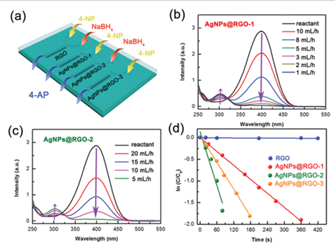
A functional microfluidic chip was formed (Figure 1a), and the closely packed AgNPs endowed the chip with catalytic capability. RGO and AgNPs@RGO‐1–3 were transferred into different channels of the chip (Figure 3a). The reduction of 4‐NP by sodium borohydride (NaBH4) was chosen as a classic reaction to evaluate the catalytic activity of AgNPs@RGO [13]. 4‐NP (6 mM) and NaBH4 (20 M) were injected into different inlets of the Y‐shaped channels. RGO-based materials can trap 4‐NP molecules via noncovalent π–π stacking interaction [14]. Reduction of 4-NP occurred only at the AgNPs@RGO region, whereby the fluid changed its color from light yellow to colorless. UV‐vis spectroscopy was used to assess the reduction efficiency of the chip as 4-NP and its reduction product 4-aminophenol (4-AP) produce characteristic absorption peaks at 400 and 295 nm, respectively. The conversion of 4-NP to 4-AP depended on the fluid velocity on the chip (Figure 3b,c). In the channel containing AgNPs@RGO‐1, 4‐NP was completely reduced at a liquid flow velocity of <1 mL h−1. This critical flow rate was defined as the threshold velocity (vth). In the channel containing AgNPs@RGO‐2, complete conversion of 4-NP occurred at a much higher vth (5 mL h−1). The difference in catalytic activity between AgNPs@RGO‐1 and -2 was due to the different contents of AgNPs and exposed active sites.
We used a pseudo‐first‐order kinetic model to investigate the catalytic performance on different substrates quantitatively [15]:
ln(C/C0) = ln(A/A0) = -kappt
where C and C0 are the real‐time and initial concentration of 4‐NP, respectively, A and A0 the corresponding absorbance intensities, and kapp the apparent first‐order reaction rate constant. Accordingly, kapp was determined to be 0.0054, 0.0207, and 0.0109 s−1 for AgNPs@RGO-1, -2, and -3 respectively, indicating that AgNPs@RGO‐2 exhibited the highest catalytic activity (Figure 3d). This result implies that laser scribing can improve the catalytic capability of AgNPs@RGO. However, the excessive amount of AgNPs in AgNPs@RGO‐3 led to the coalescence of AgNPs during laser scribing and thus to a dramatically reduced reaction rate. Therefore, microfluidic channels containing AgNPs@RGO‐2 were selected to produce practical chips.
The closely packed AgNPs on the RGO scaffold can also be used as efficient SERS sensors [16], enabling on‐chip, in situ SERS detection to directly monitor the catalytic reaction. We compared the SERS spectra of 4‐NP on different substrates. As the SERS signals are attributed to "hot spots" at the nanogaps between neighboring nanoparticles, the electric field and Raman signals were significantly enhanced on the AgNPs@RGO-1 and -2 substrates. The signal from the AgNPs@RGO‐2 substrate exhibited the greatest enhancement owing to the plasmonic effect of AgNPs and the effective interaction between 4-NP and RGO.
In practice, complete conversion of the reactant is desired; therefore, we acquired the real‐time SERS signals at the end of the channel to determine whether 4‐NP has been completely reduced. At a flow rate lower than vth, 4‐NP was almost completely converted to 4‐AP. However, at a velocity higher than vth, the product was a mixture of 4‐NP, 4‐AP, and NaBH4. These results indicate that catalytic chips with in situ SERS sensors can effectively avoid the intricate collection of the products and subsequent UV-vis measurements.
To evaluate the reproducibility of the SERS device, we collected SERS spectra of rhodamine 6G (R6G, 10−7 M) at nine randomly selected positions on the SERS sensor. Consistent signal intensities were obtained, indicating excellent reproducibility. Moreover, the SERS intensities at 1509 cm−1 were compared, and the relative standard deviation (RSD) was ≈2.3%. To test the error of concentration detection, we measured the SERS signals of R6G at different concentrations (10−5–10−10 M); the SERS intensity increased evidently with concentration. The SERS chip is also reusable. After the first SERS detection of R6G, the SERS device was regenerated with water and reused for three further detection and regeneration cycles. The signal intensity at 773 cm−1 was measured after each cycle, and the RSD was ≈6.5%, demonstrating good reusability. Furthermore, the SERS signals of devices stored for 15, 30, 45, and 60 days were measured and compared to study the shelf life of the sensor. The SERS intensity of the device stored for 60 days decreased only by 10% compared with that of a fresh device, indicating a shelf life of at least 60 days.
Conclusion
In summary, a catalytic chip with in situ SERS sensors was prepared by simple laser scribing. By adjusting the AgNPs/GO ratio, AgNPs@RGO substrates with designable structures and optimized performance were obtained. The hierarchical structures of the composites exposed numerous active sites to the environment, which contributed to the reduction of 4-NP. Due to the excellent adsorption properties of RGO and the remarkable plasmonic effect of AgNPs, the microfluidic substrates exhibit SERS sensor capability. Thus, the catalytic products could be monitored by in situ SERS detection. This cost‐effective strategy for fabricating catalytic optofluidic chips is favorable for future practical applications.
References
[1] D. Mark, S. Haeberle, G. Roth, F. von Stetten, R. Zengerle, Chem. Soc. Rev. 2010, 39, 1153.
[2] W. Xu, S. K. Paidi, Z. Qin, Q. Huang, C. H. Yu, J. V. Pagaduan, M. J. Buehler, I. Barman, D. H. Gracias, Nano Lett. 2019, 19, 1409.
[3] J. A. Huang, Y. L. Zhang, H. Ding, H. B. Sun, Adv. Opt. Mater. 2015, 3, 618.
[4] B. B. Xu, Y. L. Zhang, S. Wei, H. Ding, H. B. Sun, ChemCatChem 2013, 5, 2091.
[5] R. Dong, Y. Liu, L. Mou, J. Deng, X. Jiang, Adv. Mater. 2019, 31, 1805033.
[6] R. D. Sochol, E. Sweet, C. C. Glick, S. Y. Wu, C. Yang, M. Restaino, L. W. Lin, Microelectron. Eng. 2018, 189, 52.
[7] H. Tian, C. Li, M. A. Mohammad, Y. L. Cui, W. T. Mi, Y. Yang, D. Xie, T. L. Ren, ACS Nano 2014, 8, 5883.
[8] M. F. El‐Kady, V. Strong, S. Dubin, R. B. Kaner, Science 2012, 335, 1326.
[9] Y. S. Wang, Y. Wang, H. Xia, G. Wang, Z. Y. Zhang, D. D. Han, C. Lv, J. Feng, H. B. Sun, Nanoscale 2016, 8, 17451.
[10] W. Zhang, Y. Hu, C. Yan, D. Hong, R. Chen, X. Xue, S. Yang, Y. Tian, Z. Tie, Z. Jin, Nanoscale 2019, 11, 9053.
[11] H. Tian, Y. Yang, D. Xie, Y. L. Cui, W. T. Mi, Y. Zhang, T. L. Ren, Sci. Rep. 2015, 4, 3598.
[12] B. Han, Y. L. Zhang, Q. D. Chen, H. B. Sun, Adv. Funct. Mater. 2018, 28, 1802235.
[13] P. Liu, M. F. Zhao, Appl. Surf. Sci. 2009, 255, 3989.
[14] K. Ariga, K. Minami, L. K. Shrestha, Analyst 2016, 141, 2629.
[15] M. Nasrollahzadeh, S. M. Sajadi, A. Rostami‐Vartooni, M. Bagherzadeh, R. Safari, J. Mol. Catal. A: Chem. 2015, 400, 22.
[16] A. Balcytis, Y. Nishijima, S. Krishnamoorthy, A. Kuchmizhak, P. R. Stoddart, R. Petruskevicius, S. Juodkazis, Adv. Opt. Mater. 2018, 6, 1800292.
This text is a digest version of the following article:
Han, B., Gao, Y.‐Y., Zhu, L., Ma, Z.‐C., Zhang, X.‐L., Ding, H., Zhang, Y.‐L., In Situ Integration of SERS Sensors for On‐Chip Catalytic Reactions. Adv. Mater. Technol. 2020, 5, 1900963. https://doi.org/10.1002/admt.201900963
Source: Preview Image: matejmo/Getty Images