Laser‐Assisted, Large‐Area Selective Crystallization and Patterning of Titanium Dioxide Polymorphs
Although ubiquitous in multiple industrial applications, the widespread use of solution‐based precursors for crystalline titanium dioxide (TiO2) for optoelectronic device integration remains limited due to its high processing temperature. It is currently possible to crystallize TiO2 at lower processing temperatures, but it requires a carefully controlled atmosphere or metallic doping of the amorphous precursor and can only achieve a low‐yield conversion of the precursor. Herein, a qualitative method is presented for the processing of an amorphous photosensitive precursor to achieve high‐yield conversion to highly crystalline TiO2 at room temperature and in ambient environment using a low‐energy laser. A real potential for the additive manufacturing of TiO2 structures for photocatalysis, printable flexible hybrid electronics, and low‐cost photovoltaics using low‐energy laser processing that is compatible with heat‐sensitive materials and flexible substrates is shown. [...]
Please register below to read the full article digest.
Introduction
In recent years, careful control of the phase transition and phase stability of TiO2 polymorphs induced by low‐power visible light gained attention in the scientific community.These previous efforts all arise from the profound need for high‐quality crystalline TiO2 converted at room temperature in ambient environment. Yet, important fundamental hurdles prevent their scaling‐up to modern industrial‐like environments. In particular, the inclusion of TiO2 precursors into laser‐based 3D printers and digital inkjet printing systems, including electrohydrodynamic inkjet, has been limited by two defining factors: the high processing temperatures (beyond 400 °C) still necessary to crystallize into different polymorphs and/or the specific atmospheric conditions required to crystallize under visible light at room temperature. Both factors are highly detrimental for the widespread integration of TiO2 precursors into large volume manufacturing of many photocatalysis, energy conversion, wearable, and flexible hybrid electronic solutions.
Previously, a novel TiO2 precursor formulation has been developed relying on an incomplete nonhydrolytic sol–gel ester elimination to yield films of amorphous TiO2 suitable for laser‐induced conversion in ambient conditions. This formulation allows low‐energy laser‐induced conversion of amorphous‐to‐anatase, amorphous‐to‐rutile, anatase‐to‐rutile, or amorphous‐to‐mixture of anatase/rutile in ambient environment and at room temperature, without metallic ions or specific atmospheric conditions.
In this article, large‐scale laser‐assisted conversion of amorphous TiO2 films under ambient conditions is presented with an inexpensive approach using a low‐cost commercially available 3D printer platform with a 405 nm laser engraving attachment module to spatially control the TiO2 crystallization. To this end, it is described in detail how this unique formulation can be used to achieve selective conversion of this amorphous TiO2 into combined anatase and rutile patterns over a large surface area. The laser‐induced conversion process is carefully optimized (laser velocity, laser power setting, and number of passes) to achieve selective conversion of the TiO2 over large surface area. The morphology and integrity of the converted areas are analyzed using laser‐scanning microscopy.
Methods
The TiO2 precursor synthesis followed the procedures published in previous studies.
Optical imaging and laser 3D reconstruction were made using the Olympus Laser Confocal Microscope LEXT OLS4100.
The 3D printer of choice was the BIBO‐2 Touch printer that possesses a positional accuracy in the Z‐direction resolution of 20 μm. This accessible 3D printing system was purchased for less than 850 USD with a laser engraving module that replaced the extruder heads and was controlled by the fan TTL control circuit.
Results
A dispersion of TiO2 nanoparticles was prepared following a procedure fully described in previous studies. Pieces of standard glass slide were placed inside a plastic container containing a solution of as‐synthesized amorphous TiO2 nanoparticle suspension in hexane. The container is subsequently sealed within a box with breathing holes to avoid external contamination and, guarantee a slow and uniform evaporation of the hexane, yielding smoother films. After 12 h inside the fume hood, a densely packed film of amorphous TiO2 nanoparticles remains atop the glass after all the solvent has evaporated. The resulting film displays a reddish coloration and covers all the area of the glass as shown in Figure 1. The physical microscopic quality of the amorphous, as‐deposited film is shown in Figure 1b, and the overall look of the film atop glass is shown in Figure 1c.
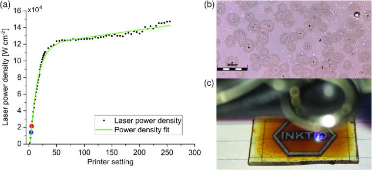
The laser head consists of a 405 nm continuous‐wave blue–violet source with a maximum 500 mW power output. At maximum power, the laser emission reaches 465 mW from the 500 mW nominal specification for the module (Figure 1a). Under low power operation, with the power control set under 50 (about 388 mW measured emission), the laser emission will not damage the unit and the impact of the poor cooling is less dramatic but, this lack of stable emission reflects in the results obtained.
Initial experiments demonstrate square areas of the film fully converted to crystalline TiO2 using the BIBO printer's laser module. Each area is filled with a simple square mesh pattern which guarantees uniform converted areas by keeping the lines close enough to each other to trigger conversion along the area of interest.
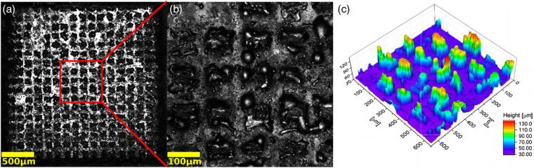
Microscopic analysis of the square patterns shows a strong penetration of the laser throughout the film to the point of complete ablation of the material, exposing the substrate, as shown in Figure 2a,b.
The main goal is to minimize this material ablation while promoting exclusively the crystallization of the amorphous TiO2 layer under environmental conditions, delivering a uniform film in which the presence of both, anatase and rutile crystalline phases is possible. Because of this unwanted material etching, lower laser power settings were explored going from 1 to 16, corresponding to power emission between 4 and 230 mW (13.7–732 W mm−2). With a new film deposited atop glass using the same described procedure, the patterns of choice are lines 100 μm thick created by doing five contiguous traces of 20 μm each (Figure 3).
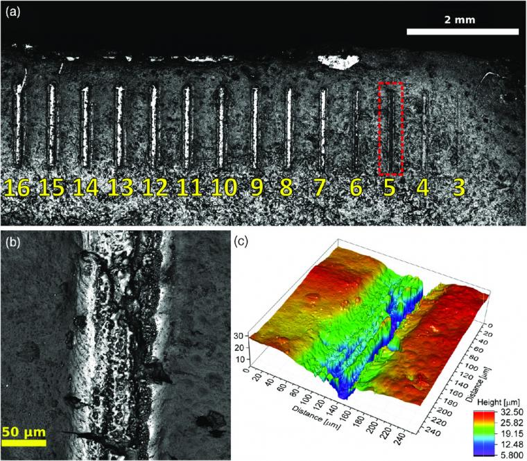
For each pattern, the power setting of the laser is fixed and ranges from 16 down to 1, in single steps. To further reduce the material displacement, the laser speed parameter was increased from 50 to 100 mm min−1. Of course, this also reduces the total dosage received by the film. The travel speed, number of passes, and pass depth remain unchanged from the previous run. From laser power setting 16 down to 6, the resulting line patterns exhibit complete crystallization to rutile. These results are like those previously obtained in the square patterns realized with higher power settings, with important material displacement and/or ablation, leaving bare areas of exposed glass where the amorphous TiO2 was previously present.
At power setting 5, the equivalent laser power density is 216 ± 10 W mm−2 (Figure 1a). At this emission power, one can already observe a smoother and more uniform, fully crystallized film (Figure 3b). The presence of cracks in the film after crystallization is largely attributed to the natural densification of the material and subsequent volume loss due to the atomic reorganization. Reported values in density for both anatase and rutile phases are 3830 and 4240 kg m−3, respectively,2 highlighting the structural differences of both phases. Indeed, the unit‐cell volume of anatase is 130.36 Å3, whereas for rutile is 62.45 Å3, factor that explains the stronger fracturing present in the rutile conversion28 when coming from an amorphous state. This fracture effect also depends on the film thickness, being more prominent in thicker films. Here, the thickness of the film used to pattern these lines is estimated to be 24 μm as shown in Figure 3c.
To showcase the endless possibilities of this TiO2 solution and low‐energy conversion process for additive manufacturing, a geometric pattern has been chosen for printing that has both rutile and anatase areas coexisting along with amorphous unconverted sections, as shown in Figure 4. In the initial pattern design, as shown in the inset in Figure 4a, there are three distinctive colors: dark brown is the amorphous film, dark gray is the anatase section, and light gray is the rutile section.
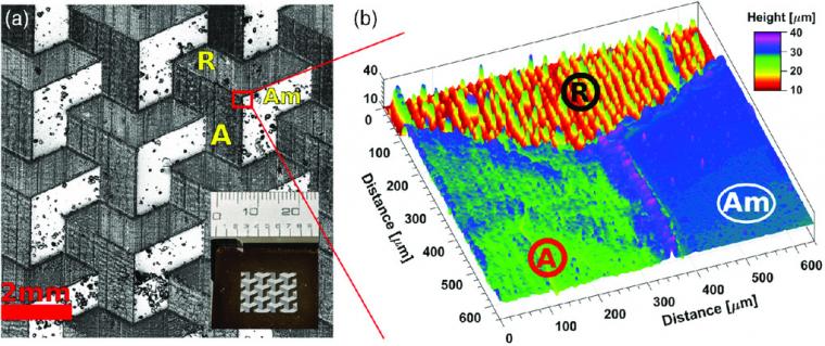
Optical characterization of the sample, shown in Figure 4b, clearly shows each section labeled (Am) amorphous, (A) anatase‐rich, and (R) rutile‐rich regions easily recognizable in this intimately dense mixed film.
It well established the advantageous and synergistic effects associated with having both phases in the same environment for photocatalytic applications. This setting reduces charge recombination boosting the degradation of organic contaminants. However, previous results require the use of two types of independent nanoparticles working together, without the level of spatial control offered here. As demonstrated by the results herein, this is the first time that a TiO2 large‐area film can be produced on‐demand where the ratio anatase:rutile is controlled directly by the geometry of each.
Discussion
Just recently, approaches that involve the use of TiO2 as part of the active material in photovoltaic applications35 and the potential of the heterojunction composed of both phases in light harvesting have just being explored. This is done using a Degussa P25 (biphasic TiO2 nanoparticles) with a fixed ratio of anatase to rutile presence in the mix. The results included in this article describe the possibility of having spatially selective biphasic TiO2 layers compatible with conventional laboratory fabrication techniques for optoelectronic devices in addition to the possibility of large‐scale production lines.
However, integration in large production lines requires more adept control of the crystallization conditions, specifically the quality and stability of the source of illumination: whether it is a low‐power laser source or a high‐power photonic curing flash lamp37 using a mask for faster, large‐area conversion. In this case, the laser unstable emission tends to variate the power delivered and creating partially converted spots in the wings. This configuration does not guarantee a uniform conversion all over the area of interest. A square profile emission present in much more expensive and reliable sources38 will increase the yield of a single crystalline phase per unit area.
Despite the low cost of the herein presented approach, good spatial resolution, control and reproducibility, the lack of proper thermal and emission stability in the laser unit makes it inappropriate to meet high‐precision industrial standards. We, however, believe this proof‐of‐concept is concrete evidence that it is possible to crystallize TiO2 under ambient environmental conditions, using a low‐cost approach, with the possibility of obtaining spatial control of the phases by only adjusting the emission parameters of a laser source.
Conclusions
As a wide bandgap semiconductor, TiO2 is an attractive candidate, especially for application into dye‐sensitized solar cells (DSSCs) where the light absorption role and the charge transport role are separated. The integration of TiO2 in novel organic and inorganic photovoltaic devices is limited to a charge transporting role due to the incompatibility of the crystallization process of TiO2 that damages the other materials involved in the fabrication of the device. Crystallized TiO2, whether as anatase (3.2 eV bandgap) or rutile (3.0 eV bandgap), exhibits optical absorption at the violet portion of the optical spectrum, and with this technique, it is possible to fabricate and integrate devices that take full advantage of this asset.
By utilizing a defect‐rich synthesis of nonhydrolytic TiO2 that shows enhanced sensibility to photoconversion while avoiding costly and lengthy thermal crystallization procedure, it is demonstrated that it is possible to have large‐area deposition and conversion of biphasic thin layers of TiO2. Complete area‐selective conversion to either anatase or rutile is possible, while preserving the state of the other one.
In addition to create fully crystallized large‐area patterns with “a la carte” ratio of each phase, it is now possible to experiment with unconventional patterns between these two phases. In addition, this improvement brings new possibilities for low‐cost printed flexible electronics, wearable devices, and novel additive manufacturing schemes. Most importantly, with the presented approach, this procedure could be automated and repeated by a machine learning platform for large‐scale production of devices.
Source: Preview Image: Jürgen Fälchle/stock.adobe.com