Thin Film Characterization
This brief introduction will discuss some of the techniques to characterize thin films. The methods are characterized by their distinct operating prin- ciples, namely mechanical characterization techniques, thermal analyses, scanning probe methods, and methods that involve the interaction of radiation (e.g., electrons, ions, and photons) with matter. The introduction will highlight laser scanning confocal microscopy as a promising method to characterize the morphology of a wide variety of thin-film materials.
Thin film technology is ubiquitous across materials science for applications such as semiconductors,[1,2] electronics (e.g., light-emitting diodes, soft electronics),[2,3] microelectromechanical systems (MEMS),[4] memory devices,[2,5] energy storage (batteries, capacitors),[6,7] photovoltaics,[8,9] fuel generation,[10] catalysis,[11] chemical sensors,[12,13] environmental coat ings (e.g., thermal),[14] chemical barriers (e.g., diffusion, corrosion),[15,16] radiation detection,[2] photodetectors,[17] microfluidics,[18] piezoelectric devices,[19] mechanical layers (e.g., adhesion, lubrication, hardness),[20–22] magnetic devices (e.g., SQUID),[23] optical coatings (e.g., electrochromic, antireflection, interference, waveguides),[24] biomaterials and biomedical applications,[25] and many more. Furthermore, there are sufficient fabrication techniques that virtually any type of material can be prepared as a thin film, such as metals, alloys, oxides, ceramics, glasses, polymers, inorganic complexes, organic molecules, and biological molecules.
The ability to prepare a material into a thin film can enable specific material properties and unlock particular applications. Often, the nano-, micro-, and millimeter-scale morphologies of the thin film have import- ant implications on its properties and eventual application. Therefore, the characterization of the morphology of thin films is an integral part of materials science research. There are a variety of different characteriza- tion techniques with different pros and cons in terms of resolution, the field of view, sample size, ease of use, speed, and information that can be obtained.
This brief introduction will discuss some of the techniques to characterize thin films. The methods are characterized by their distinct operating principles, namely mechanical characterization techniques, thermal analyses, scanning probe methods, and methods that involve the interaction of radiation (e.g., electrons, ions, and photons) with matter. The introduction will highlight laser scanning confocal microscopy as a promising method to characterize the morphology of a wide variety of thin-film materials.
Mechanical Characterization
The mechanical properties of a thin film can provide information on the underlying morphology of the material. The manner in which a thin film responds to a particular mechanical deformation is dependent on the assembly of its constituent components. Furthermore, the influence of volumetric and interfacial constraints can cause mechanical properties to differ from bulk values. Cantilever beam or plate type structures are commonly used to measure residual stress, from deflection and curvature measurements. The Young’s modulus and plastic properties of thin films can be determined by analyzing the stress associated with thermal cycling using thin wafer or cantilever beam measurements. Elastic moduli and other mechanical properties of thin films can be measured by cantilever beam resonant frequency methods. Furthermore, measurement techniques such as microindentation and substrate curvature can be utilized to determine the plastic properties of submicron thin films and multilayers on substrates. Peel, pull, and scratch tests are used to characterize the adhesion properties of materials; however, they do not provide quantitative information regarding interfacial atomic bonding strength. Lastly, microindentation and micro-scratch characterization methods can provide a further understanding of the mechanical processes of thin films.[26]
Thermal Characterization
The thermal properties of materials can also shed light on the underlying morphology of thin films. Thermal characterization can provide physical and chemical information of the thin film.[27] Thermogravimetric analysis (TGA) is used to measure the mass change of a sample as a function of temperature. The off-gas from TGA experiments can be analyzed by mass spectrometry (MS) and Fourier transform infrared spectroscopy (FTIR) to understand the chemistry of the thermal decomposition products.[28] Differential thermal analysis (DTA) measures the temperature differences between a sample and a reference as they are simultaneously heated or cooled, whereas differential scanning calorimetry (DSC) measures the difference in heat flow. Both DTA and DSC can be used to determine properties such as the crystallinity, glass transition, phase changes, chemical reactions, heat capacity, etc.[27,29] Finally, dynamic infrared thermography can be used to determine the thermal conductivity, heat capacity, and thermal diffusivity of thin films.[30]
Scanning Probe Characterization
Physical probes can be used to scan the surface of thin films to understand both their surface and, to some extent, their bulk morphologies. Surface profilometry is a useful tool for measuring the thickness, roughness, and texture of thin films. In profilometry, a stylus probe is brought into direct contact with the film, and a line scanis performed.[31] In atomic force microscopy (AFM), a sharp probe is raster-scanned across a sample surface, in contact or non-contact modes. Interaction forces between the sample and the probe are measured by the deflection of the cantilever containing the probe and used to generate an image.[32] Different force modes can be analyzed, such as attractive, repulsive, magnetic, electrostatic, and van der Waals.
In certain thin conductive films, bulk morphologies can be constructed using conductive AFM (cAFM).[33] Also, Kelvin probe force microscopy (KPFM) can be used to measure charge accumulation[34] and the work function of thin films.[35] Although AFM is capable of sub-nm resolution and is nondestructive, it is not rapid, it is susceptible to artifacts, and has difficulties capturing large variations in sample thickness.[36] Scanning electrochemical microscopy (SECM) uses an ultramicroelectrode tip and can be used to map the electrochemical activity of a thin film.[37] Finally, scanning tunneling microscopy (STM) utilizes a metallic probe which is scanned over a thin film, and a voltage is applied between the tip and the surface. In this way, the quantum tunneling current is used to image the sample.[38] STM can achieve angstrom-scale resolution but requires specialized vacuum equipment.
Electron Microscopy
Transmission electron microscopy (TEM) can be used to elucidate the structure, chemistry, and properties of thin films. In TEM, the transmission of an electron beam through a sample is used to generate an image. Since electrons interact strongly with matter, both structural and chemical information can come from TEM characterization. Additional techniques in TEM include selected area electron diffraction (SAED), electron energy loss spectroscopy (EELS), and energyfiltered TEM (EFTEM). In TEM, due to the small de Broglie wavelength of electrons, the lattice spacing of atoms can be imaged. The sample requires special preparation and must be very thin so that the electron beam is not attenuated by the sample, and special vacuum equipment is required.[39] Meanwhile, in scanning electron microscopy (SEM), an electron beam is raster-scanned over a sample, and either secondary electrons or backscattered electrons from the sample are detected to map the sample topology. SEM has a wider field of view than TEM, and it does not require ultrathin samples because it does not rely on electrons being transmitted through the sample; however, the resolution of SEM is less than TEM, around 1 nm.
Further, energy-dispersive X-ray spectroscopy (EDS) can be used to spatially map the elemental content of thin films. Also, the orientation and phase of crystalline domains can be determined by the diffraction of backscattered electrons (EBSD).[40]
Ion Beam Techniques
Helium ion microscopy (HeIM) is an imaging technique similar to SEM, but instead of an electron beam, a helium ion beam is scanned over the sample. Secondary electrons ejected from the sample due to the impact of helium ions are detected. The HeIM beam can be less than 1 nm, enabling high resolution with a fairly wide field of view.[41] In another method, elemental maps of thin films can be constructed by time-of-flight secondary ion mass spectrometry, where a pulsed ion beam is scanned over a sample, which removes particles from the surface that are detected by MS.[42]
X-ray-based Techniques
The interaction of X-rays (and neutrons, which is not discussed here) with matter is a useful tool to determine thin film morphology. Small-angle X-ray scattering (SAXS) characterization of a thin film, either in transmission or grazing incidence (i.e., GISAXS) configurations,[43] can give information on the periodic structures in the film at the nanometer scale. Whereas, X-ray diffraction (XRD) and wide-angle X-ray scattering can provide structural information at the angstrom-scale.[44] Soft/resonant X-rays can be used to probe particular chemical groups in the material.[45] Furthermore, X-ray reflectivity (XRR) is a useful tool for determining the thickness of thin films.
[46] Lastly, X-ray microtomography (µCT) uses X-rays to create cross-sections of samples, which can be constructed into 3D images.[47]
Photon-based Methods
Optical microscopy (OM) is one of the oldest methods to determine a sample’s morphology, dating back to the seventeenth century. OM is one of the most important techniques for identifying features > 500 nm in materials and thin films. Particular techniques in OM include brightfield, darkfield, polarization, interference, and phase-contrast microscopies. Contrast in OM is created by various mechanisms, depending on the imaging mode, such as absorption of light, scattering, rotation of polarized light, and interference.[48] Lastly, near-field scanning optical microscopy (NSOM) is a technique where nanoscale morphologies can be elucidated by scanning a small fiber-optic probe over thin films. When the distance between the probe and the sample is smaller than the wavelength of light, the resolution of the image is not limited by the optical wavelength.[49] Finally, confocal microscopy has several advantages over conventional widefield OM, such as the ability to control depth of field, elimination or reduction of background information, and the capability to collect serial optical sections from specimens.[36,48,50] In particular, laser confocal scanning microscopy will be discussed in the next section.
Laser Confocal Scanning Microscopy
In far-field optical techniques, imaging is accomplished by focusing elements. In a microscope, the objective lens forms a magnified image of the illuminated object that can then be examined with the eyepiece. If we consider the image of a single point, the light intensity is distributed around the focal point in a focal volume described by a point spread function (PSF). The extent of the PSF determines the resolution. In the ideal case where no aberrations are present, the resolution is limited by diffraction and is determined by the wavelength of light in the medium (ln) and the aperture angle of the lens NA=n sin(u), where n is the refractive index of the medium and u is the half-angle of the lens aperture, and can be expressed by the Rayleigh theoretical resolution limit : RL=0.61l ⁄NA. Much research has been devoted to developing tools able to image objects with a resolution lower than the Rayleigh limit. By confocal microscopy, a resolution about 30% less than the Rayleigh limit is obtained. This considerable advantage of confocal microscopy follows by the use of a point detector, obtained in practice by placing a circular pinhole in front of the photodetector that cuts off the out-offocus light from surrounding planes.[36]
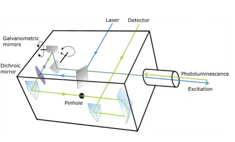
Although the confocal microscope was invented in 1955 by Minsky,[51] it was not widely adopted until the invention of lasers and the availability of high-performance computing. Laser scanning confocal microscopes (LSCMs) use collimated laser light as a ‘point’ illumination source, with point focus on the sample, and focus the reflected, transmitted, or fluoresced light through a pinhole to provide a ‘point’ detector. A schematic of the laser scanning head is shown in Figure 1.[50]
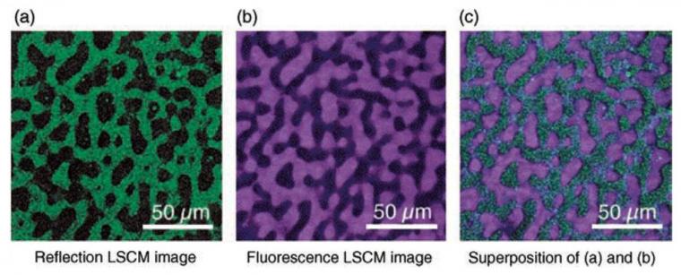
Multiple imaging detection modes can be used with LSCM, including but not limited to reflected light, transmitted light, fluorescence, and Raman spectroscopy. The different imaging modes can provide different information about the thin film, and the different modes can be superimposed to create a composite image of the sample (Figure 2).[48] As long as surface topology is the only characterization needed, reflection mode can be an ideal method to characterize thin films.[52] One benefit of reflection mode for materials science is that the material does not need to be fluorescent to be imaged; this is ideal for many materials systems. Thus, as-prepared samples can easily be characterized. For reflected light imaging, the smallest available wavelength laser (e.g., 405 nm) is optimal, as the optical resolution is directly proportional to wavelength.[50] The high spatial resolution, wide field of view, minimal sample preparation, relative ease of measurement (i.e., no vacuum equipment required), the ability to characterize samples that have large height variation, the ability to construct 3D and pseudo-infinite depth of field imaging, and versatility (i.e., material selection and imaging modes) of LSCM make it an ideal tool of characterizing the morphology of thin films in materials science.
References:
[1] E. Fortunato, P. Barquinha, R. Martins, Adv. Mater. 2012, 24, 2945.
[2] Z. Wang, P. K. Nayak, J. A. Caraveo-Frescas,
H. N. Alshareef, Adv. Mater. 2016, 28, 3831.
[3] M. Kim, C. Kim, H. Alrowais, O. Brand, Adv. Mater. Technol. 2018, 3, 1800061.
[4] S. Trolier-McKinstry, P. Muralt,
J. Electroceramics 2004, 12, 7.
[5] D. B. Strukov, G. S. Snider, D. R. Stewart,
S. R. Williams, Nature 2008, 453, 80.
[6] S. Moitzheim, B. Put, P. Vereecken, Adv. Mater. Interfaces 2019, 6, 1900805.
[7] M. Yu, X. Feng, Joule 2019, 3, 338.
[8] B. Kippelen, J.-L. Brédas, Energy Environ. Sci. 2009, 2, 251.
[9] S. Sundaram, K. Shanks, H. Upadhyaya, “Thin Film Photovoltaics” in A Comprehensive Guide to Solar Energy Systems 2018, 361.
[10] R. Shwetharani, H. R. Chandan, M. Sakar, G. Balakrishna, K. Reddy, A. Raghu, Int. J. Hydrog. Energy 2019.
[11] C. Guizard, A. Princivalle, Catal. Today 2009, 146, 367.
[12] H. Mukamal, S. Cordero, D. Ruiz, M. Beshay,
R. Lieberman, Proc. SPIE 2005, 6004, 600406.
[13] C. Mackin, A. Fasoli, M. Xue, Y. Lin, A. Adebiyi,
L. Bozano, T. Palacios, 2D Mater. 2020, 7, 022002.
[14] J. Thakare, C. Pandey, M. Mahapatra,
R. Mulik, Met. Mater. Int. 2020, 1.
[15] L. H. Hihara, “Electrochemical aspects of corrosion-control coatings” in Intelligent Coatings for Corrosion Control 2015, 1.
[16] L. Körner, A. Sonnenfeld, P. Rohr, Plasma Process. Polym. 2009, 6, S660.
[17] Z. Han, H. Liang, W. Huo, X. Zhu, X. Du, Z. Mei, Adv. Opt. Mater. 2020, 8, 1901833.
[18] M. Focke, D. Kosse, C. Müller, H. Reinecke,
R. Zengerle, F. Stetten, Lab Chip 2010, 10, 1365.
[19] A. Khan, Z. Abas, H. Kim, I.-K. Oh, Smart Mater. Struct. 2016, 25, 053002.
[20] S. Mishra, D. Verma, S. Bysakh,
L. Pathak, J. Nanomater. 2013, 2013, 1.
[21] S. Lučić, V. Kovačević, D. Hace, Int. J. Adhes. Adhes. 1998, 18, 115.
[22] E. W. Roberts, Tribol. Int. 1990, 23, 95.
[23] G. Ehnholm, T. Wiik, T. Stubb, Jpn. J. Appl. Phys. 1977, 16, 261.
[24] A. Piegari, F. Flory, Optical thin films and coatings: From materials to applications; 2018.
[25] H. Griesser, Thin film coatings for biomaterials and biomedical applications; 2016.
[26] P. S. Alexopoulos, T. C. O’Sullivan, Annu. Rev. Mater. Sci. 1990, 391.
[27] A. W. Coats, J. P. Redfern, Analyst 1963, 88, 906.
[28] L. Renna, F.-G. Blanc, V. Giordani,
J. Electrochem. Soc. 2020, 167, 070542.
[29] M. Yu. Efremov, J. T. Warren, E.
A. Olson, M. Zhang, A. T. Kwan, L. H. Allen, Macromolecules 2002, 35, 1481.
[30] A. Greppmair, N. Galfe, K. Amend,
M. Stutzmann, M. Brandt, Rev. Sci. Instrum. 2019, 90, 044903.
[31] M. Tosa, “Surface Profilometer” in Compendium of Surface and Interface Analysis 2018, 679.
[32] G. Friedbacher, “Atomic Force Microscopy (AFM)” in Surface and Thin Film Analysis:
A Compendium of Principles, Instrumentation, and Applications, Second Edition 2011, 443.
[33] L. A. Renna, M. Bag, T. S. Gehan, X. Han,
P. M. Lahti, D. Maroudas, D. Venkataraman, J. Phys. Chem. B 2016, 120, 2544.
[34] L. A. Renna, Y. Liu, T. P. Russell, M. Bag,
D. Venkataraman, Mater. Lett. 2018, 217, 308.
[35] V. Palermo, M. Palma, P. Samorì, Adv. Mater. 2006, 18, 145.
[36] M. A. Loi, E. D. Como, Michele, “Morphology-Correlated Photophysics in Organic Semiconductor Thin Films by Confocal Laser Microscopy and Spectroscopy” in Photophysics of Molecular Materials: From Single Molecules to Single Crystals 2005, 153.
[37] G. Lu, J. Cooper, P. McGinn, Electrochim. Acta 2007, 52, 5172.
[38] L. Yue, C. Xiangzhen, W. Runwen, Microw. Opt. Technol. Lett. 1989, 2, 135.
[39] A. Petford-Long, A. Chiaramonti, Annu. Rev. Mater. Res. 2008, 38, 559.
[40] M. Johnson, C. Carter, J. Michael, J. Am. Ceram. Soc. 1999, 82, 1644.
[41] A. Pearson, S. Boden, D. Bagnall, D. Lidzey,
C. Rodenburg, Nano Lett. 2011, 11, 4275.
[42] D. Mao, G. Blatz, C. E. Wickersham,
M. Gloeckler, Sol. Energy Mater. Sol. Cells 2016, 157, 65.
[43] S. H. Kim, M. J. Misner, T. Xu, M. Kimura,
T. P. Russell, Adv. Mater. 2004, 16, 226.
[44] A. Hexemer, W. Bras, J. Glossinger,
E. Schaible, E. Gann, R. Kirian, A. MacDowell,
M. Church, B. Rude, H. Padmore, J. Phys.: Conf. Ser. 2010, 247, 012007.
[45] G. M. Su, W. White, L. A. Renna, J. Feng,
S. Ardo, C. Wang, ACS Macro Lett. 2019, 8.
[46] T. P. Russell, Mater. Sci. Rep. 1990.
[47] A. Hierro-Rodriguez, C. Quirós, A. Sorrentino,
L. M. Alvarez-Prado, J. I. Martín, J. M. Alameda,
S. McVitie, E. Pereiro, M. Vélez, S. Ferrer, arXiv prepr. arXiv 2019, 1907.01261.
[48] M. Ramanathan, S. B. Darling, “Optical Microscopy (Polarized, Interference, and PhaseContrast Microscopy) and Confocal Microscopy” in Characterization of Polymer Blends: Miscibility, Morphology, and Interfaces 2014, 523.
[49] P. F. Barbara, D. M. Adams, D. B. O’Connor, Annu. Rev. Mater. Sci 1999, 29, 433.
[50] D. B. Hovis, A. H. Heuer, J. Microsc. 2010, 240, 173.
[51] M. Minsky, Scanning 1996.
[52] A. Ribbe, M. Hayashi, M. Weber,
T. Hashimoto, Polymer 1998, 39, 7149.
Source: Preview Image: MMassel/Getty Images